Single chip microcomputer having a dedicated address bus and dedicated data bus for transferring register bank data to and from an on-line RAM

a single chip, register bank technology, applied in the field of single chip microcomputers, can solve the problems of reducing system performance, requiring a large space for multi-port general purpose register sets, and consuming a large amount of memory, so as to achieve efficient use of chip space and facilitate data transfer.

Inactive Publication Date: 2001-04-24
KK TOSHIBA
View PDF8 Cites 105 Cited by
  • Summary
  • Abstract
  • Description
  • Claims
  • Application Information

AI Technical Summary

Benefits of technology

is to provide a single chip microcomputer employing a register bank method. This microcomputer effic

Problems solved by technology

Generally, the external memory is accessible only at low speed, so that it takes a very long time for saving and restoring data of the registers to and from the external memory.
This is a bottleneck for the built-in control devices that must quickly respond to an interrupt request in real time, and lowers system performance.
As the number of the register banks increases, the conventional register bank method has raised the following problems.
Namely, the multiport general purpose register set inevitably needs a large space.
In addition, the multiport memory involving a large number of bits is difficult to design, consumes a lot of power, and operates at slow speed.
The conventional register bank memories must use multiport memory cells, so that, when the number of register banks is increased, its portion of the chip space greatly increases and large electric power is cons

Method used


Image

  • Single chip microcomputer having a dedicated address bus and dedicated data bus for transferring register bank data to and from an on-line RAM
  • Single chip microcomputer having a dedicated address bus and dedicated data bus for transferring register bank data to and from an on-line RAM
  • Single chip microcomputer having a dedicated address bus and dedicated data bus for transferring register bank data to and from an on-line RAM

Examples


Embodiment Construction

The embodiments of the invention will be explained with reference to the drawings.

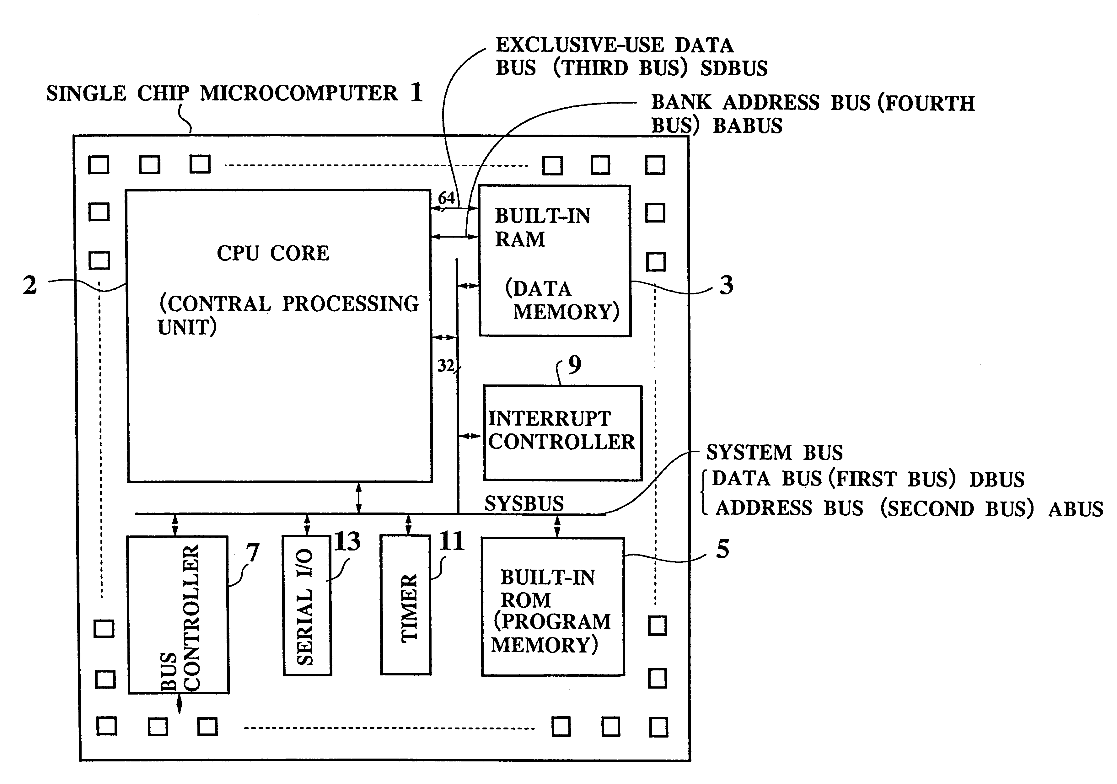
FIG. 3 shows a single chip microcomputer according to the first embodiment of the invention.

The single chip microcomputer 1 comprises a CPU (central processing unit) core 2, a on-chip RAM (data memory) 3, a on-chip ROM (program memory) 5, a bus controller 7, an interrupt controller 9, a timer 11, and a serial I / O 13. These elements receive and transmit data through a 32-bit system bus SYSBUS (involving a 16-bit address bus ABUS,and a 16-bit data bus DBUS) disposed in the chip. Data to and from the outside of the chip are passed through a bus controller 7 and an I / O pad.

According to one of the features of the invention, the CPU core 2 is connected with the RAM 3 through exclusive-use buses, which include a 64-bit bidirectional data bus SDBUS and an 8-bit bank address bus BABUS for indicating an address in the RAM 3.

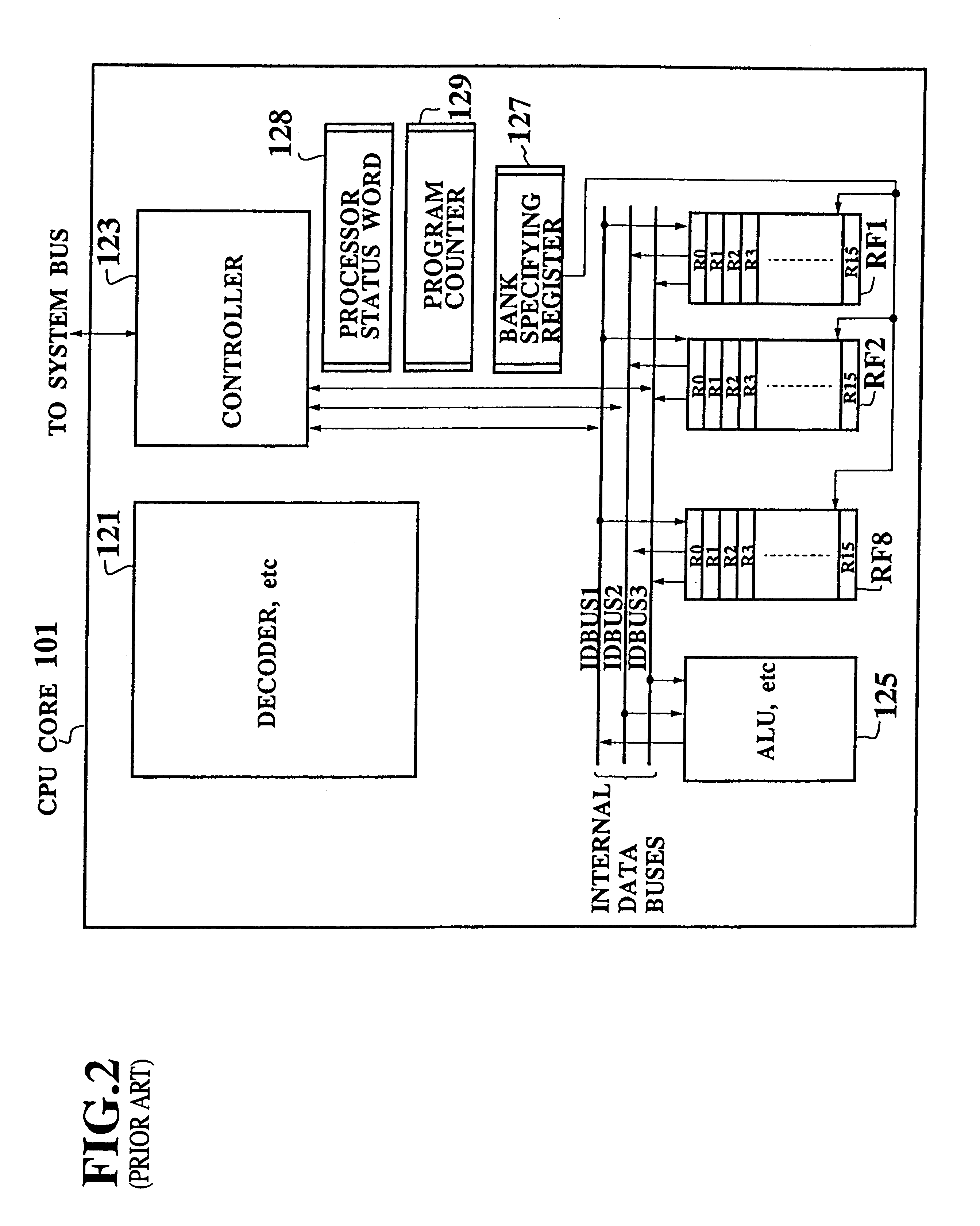
FIG. 4 shows the inside of the CPU core 2. The CPU core 2 includes a general purpose regi...


PUM


Abstract

A single chip microcomputer comprises a central processing unit (CPU) 2, a on-chip RAM 3, a on-chip ROM 5, a first bus DBUS for connecting the CPU, RAM, and ROM with one another and transferring data between them, a second bus ABUS for passing address data corresponding to the data passed through the first bus, a third bus SDBUS for connecting the CPU 2 with the RAM 3 and transferring data between them, the number of bits of the third bus SDBUS being larger than that of the first bus DBUS, and a fourth bus BABUS for connecting the CPU 2 with the RAM 3 and passing address data corresponding to the data passed through the third bus SDBUS. The CPU 2 has a data memory RF serving as general purpose registers for providing internal data to the third bus SDBUS, and a bank specifying register BP for holding positional data of a mapping region in the RAM 3 where the contents of the data memory RF are mapped and providing the positional data to the fourth bus BABUS. The RAM 3 has a memory cell array 31, a bank address control circuit 35 connected to the fourth bus BABUS, for generating a real address according to the contents of the bank specifying register BP (BP0, BP1), and a selection circuit 37 for selecting the real address generated by the bank address control circuit 35, or the address provided through the second bus ABUS.

Description

1. Field of the InventionThe present invention relates to a single chip microcomputer, and particularly to a high-speed single chip microcomputer which is compact and has a register bank function to form a high-performance system.2. Description of the Prior ArtGeneral purpose microcomputers (MCUs) and microprocessors (MPUs) used for built-in control devices usually employ a register bank function to process interrupts at high speed or to deal with multitasking and multiprogramming systems.The MCUs and MPUs usually incorporate a set of general purpose registers (for example, eight 16-bit registers), a program counter, and a processor status word. These registers are selected by a user program and used for holding various data such as operation results and program statuses.When an interrupt occurs to execute an interrupt processing program, or when a request (task switch) for executing an urgent program arises under a multitask environment, or when a subroutine call occurs for shiftin...

Claims


Application Information

Patent Timeline
IPC IPC(8): G06F15/78G06F15/76G06F9/46
CPCG06F9/462G06F15/7842G06F17/00
Inventor NISHIMURA, AKIRAOGAWA, SUNAOYAMADA, YASUOKANUMA, AKIRA
Owner KK TOSHIBA
Why Eureka
Try Eureka