Semiconductor device with a modulated gate oxide thickness

a technology of gate oxide thickness and semiconductor device, which is applied in the direction of semiconductor device, basic electric element, electrical apparatus, etc., can solve the problems of reducing production throughput, reducing the efficiency of manufacturing, and escalating the requirements for high density and performance associated with ultra large-scale integration semiconductor devices. achieve the effect of reducing drain capacitance and high reliability

Inactive Publication Date: 2001-05-08
GLOBALFOUNDRIES INC
View PDF2 Cites 28 Cited by
  • Summary
  • Abstract
  • Description
  • Claims
  • Application Information

AI Technical Summary

Benefits of technology

An advantage of the present invention is a semiconductor device comprising a transistor exhibiting reduced drain capacitance and a gate oxide layer with high reliability.
Embodiments of the present invention include a semiconductor device comprising a transistor with a gate oxide layer having a thickness which gradually increases from proximate the drain region to proximate the source region, and a gate oxide having a first uniform thickness and a second uniform thickness greater than the first uniform thickness with a gradually increasing the transition zone between the first thickness and the second thickness. Embodiments of the present invention also include thermally oxidizing a substrate surface to form a gate oxide layer having a modulated thickness by ion implanting neutral impurities, such as silicon, argon or germanium, to increase the substrate surface oxidation rate proximate the contemplated source region and / or ion implanting nitrogen into the substrate surface to reduce the oxidation rate proximate the contemplated drain region.

Problems solved by technology

The escalating requirements for high density and performance associated with ultra large scale integration semiconductor devices have been found difficult to satisfy in terms of providing a low RC (resistance capacitance) interconnection pattern.
As design rules are reduced to about 0.18 micron and below, e.g., about 0.15 micron and below, the rejection rate due to integrated circuit speed delays severely limits production throughput and significantly increases manufacturing costs.
Conventional integrated circuits are limited in speed by a high capacitance load.

Method used


Image

  • Semiconductor device with a modulated gate oxide thickness
  • Semiconductor device with a modulated gate oxide thickness
  • Semiconductor device with a modulated gate oxide thickness

Examples


Embodiment Construction

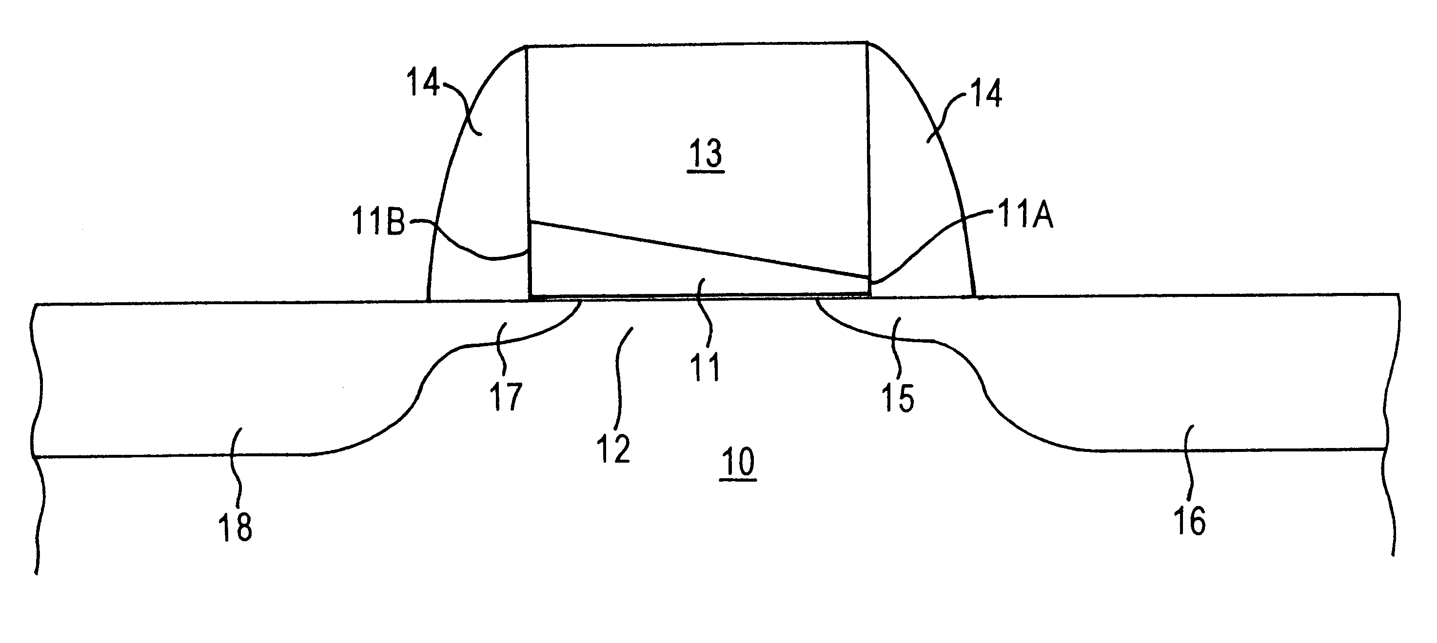
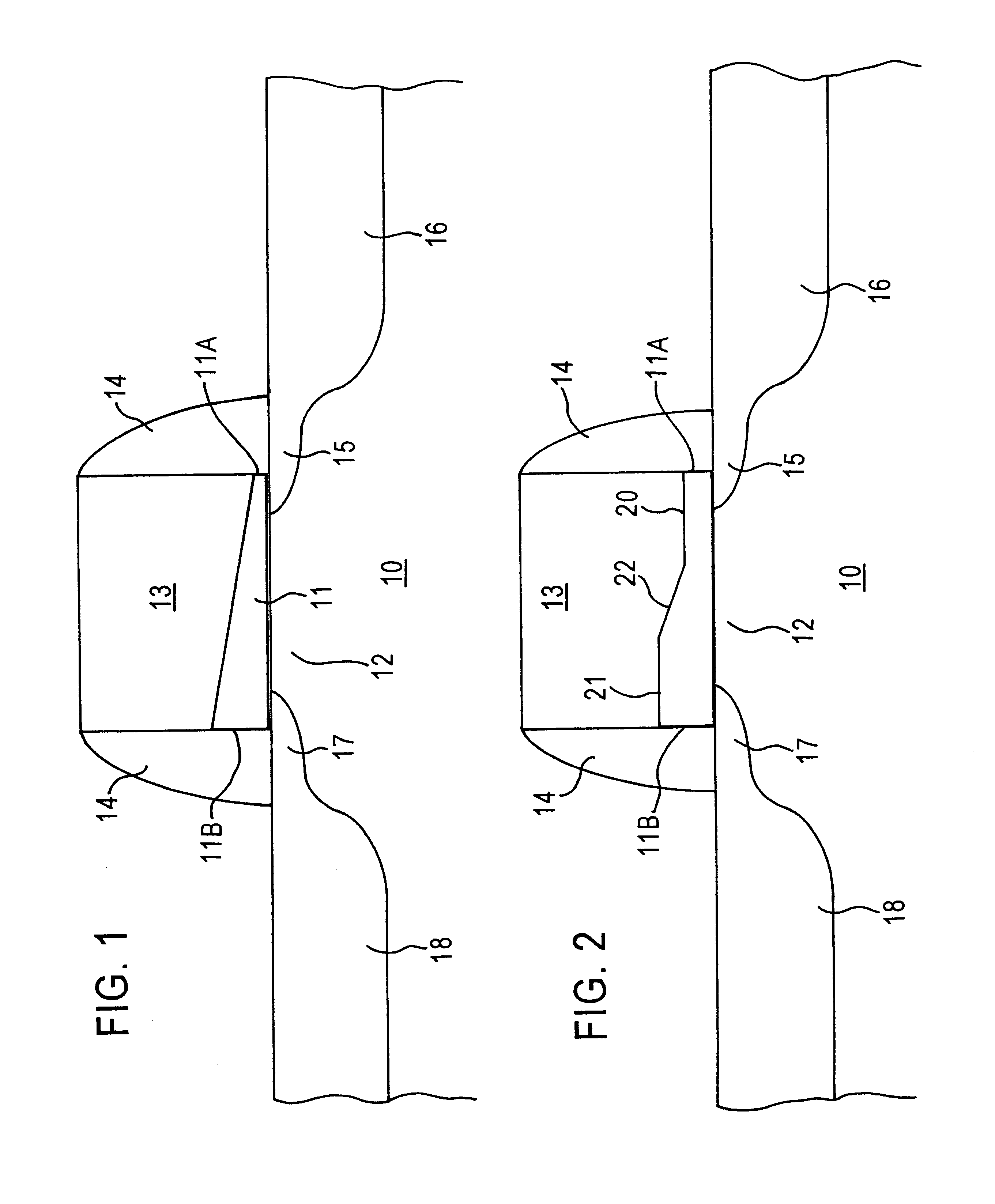
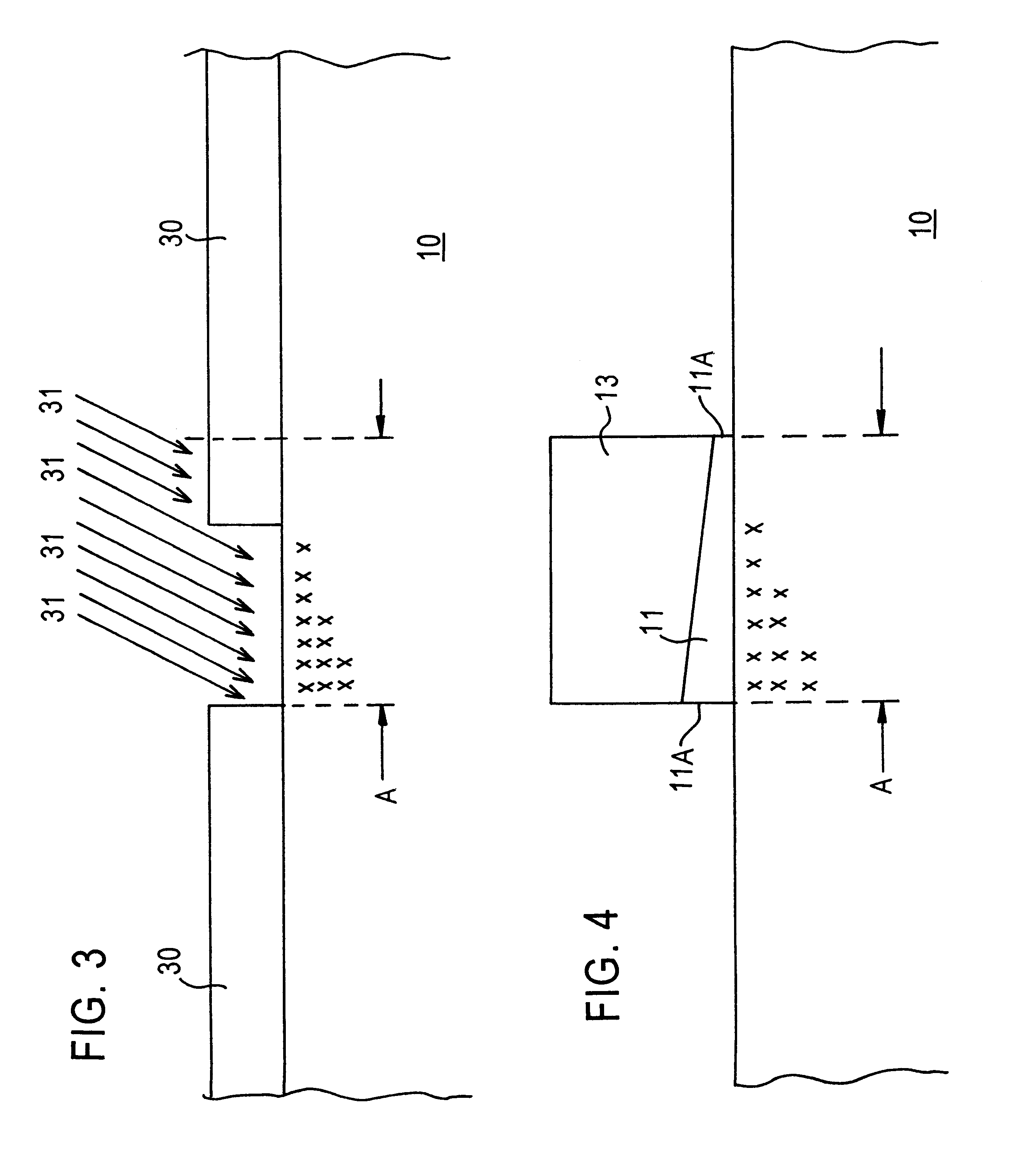
The present invention addresses and solves problems attendant upon attempting to satisfy the speed requirements for semiconductor circuitry as feature sizes are reduced into the deep sub-micron ranges to satisfy the increasing demands for miniaturization. Thus, the present invention enjoys particular industrial applicability in manufacturing semiconductor devices having a design rule of about 0.18 micron and under, e.g., about 0.15 micron and under. The present invention advantageously reduces drain capacitance without creating reliability problems attendant upon reduction of the gate dielectric layer thickness.

The present invention achieves the foregoing objectives by strategically decoupling the thickness of the gate dielectric layer proximate the drain region from the thickness of the gate dielectric layer proximate the source region. Thus, the present invention provides a gate dielectric layer with a modulated thickness strategically optimized in proximity to the drain region fo...


PUM


Abstract

High drain capacitance is reduced, thereby increasing device speed, by forming transistors with a gate oxide having a thickness which is smaller at the drain region than at the source region. Embodiments include selectively ion implanting neutral impurities, such as silicon, geranium or argon, into and / or roughening the substrate surface to increase its oxidation rate proximate the contemplated source region and / or selectively ion implanting nitrogen to reduce its oxidation rate proximate the contemplated drain region. Other embodiments include etching a gate oxide layer having a first thickness to form a portion having a reduced second thickness proximate the contemplated drain region and thermally oxidizing to form a transition zone having a thickness gradually decreasing from the first thickness to the second thickness.

Description

The present invention relates to a semiconductor device suitable for high speed performance. The present invention is particularly applicable for ultra large scale integration semiconductor devices having a design rule of abut 0.18 micron and under.1. Background ArtThe escalating requirements for high density and performance associated with ultra large scale integration semiconductor devices have been found difficult to satisfy in terms of providing a low RC (resistance capacitance) interconnection pattern. High performance microprocessor applications require rapid speed of semiconductor circuitry. The speed of semiconductor circuitry various inversely with the resistance and capacitance of the interconnection pattern. As design rules are reduced to about 0.18 micron and below, e.g., about 0.15 micron and below, the rejection rate due to integrated circuit speed delays severely limits production throughput and significantly increases manufacturing costs.Conventional integrated circu...

Claims


Application Information

Patent Timeline
Patent Type & Authority Patents(United States)
IPC IPC(8): H01L21/28H01L21/02H01L29/423H01L29/40H01L21/265H01L29/51
CPCH01L21/28202H01L21/2822H01L29/42368H01L29/518H01L21/26586
Inventor RICCOBENE, CONCETTA
Owner GLOBALFOUNDRIES INC
Why Eureka
Try Eureka