

Process for producing a sealing and mechanical strength ring between a substrate and a chip hybridized by bumps on the substrate
- Summary
- Abstract
- Description
- Claims
- Application Information
AI Technical Summary
Benefits of technology
Problems solved by technology
Method used
Image

Examples
Embodiment Construction
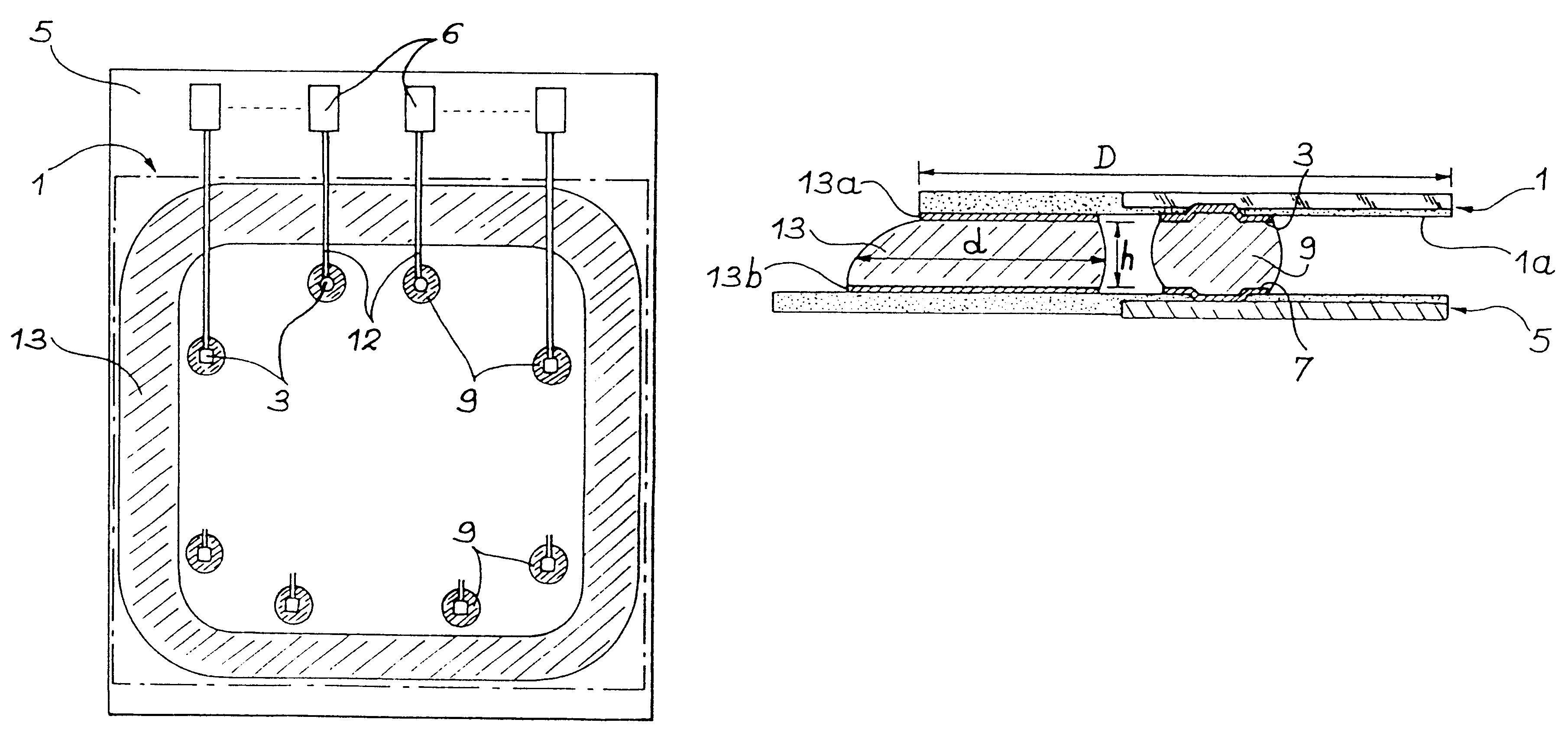
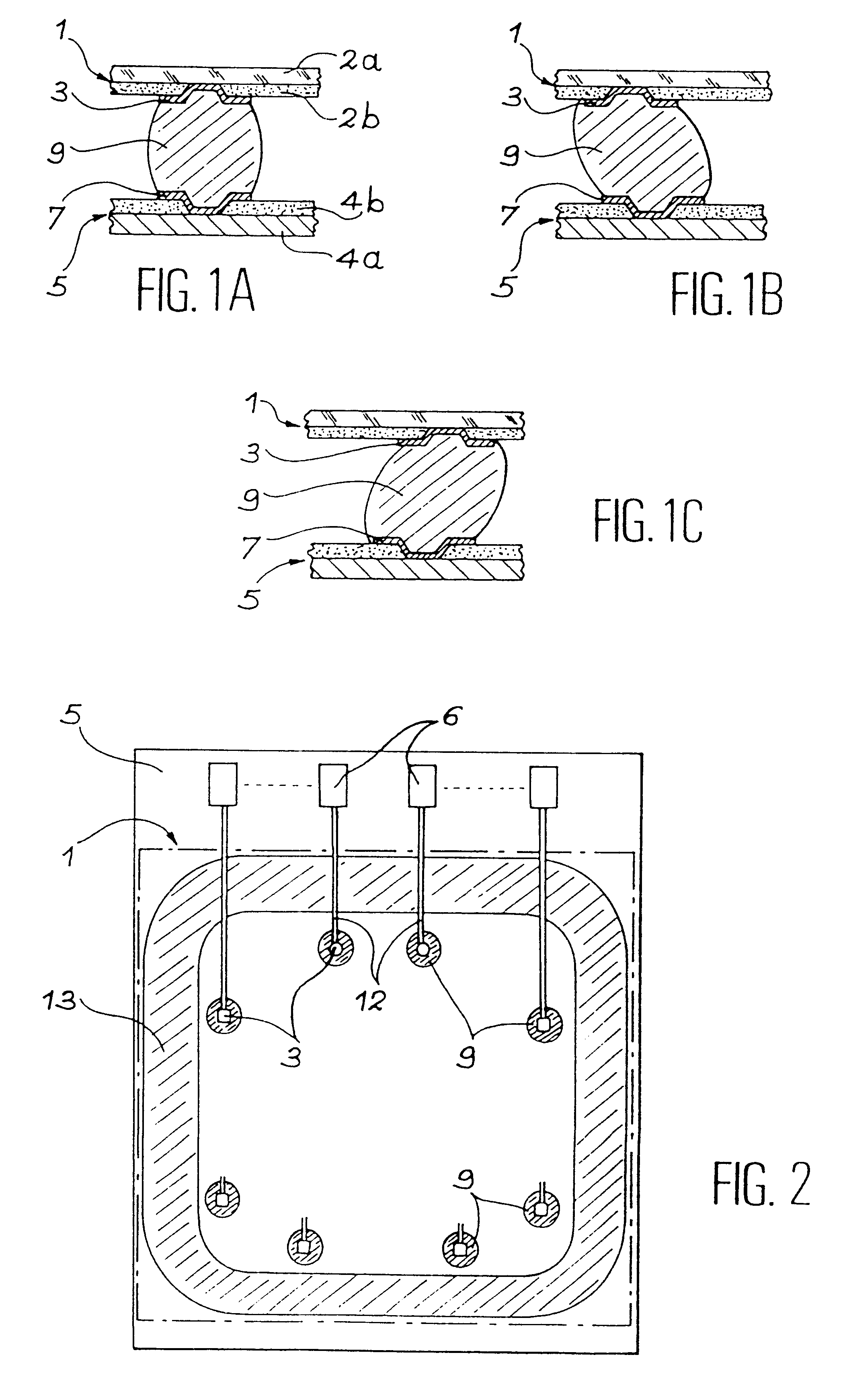
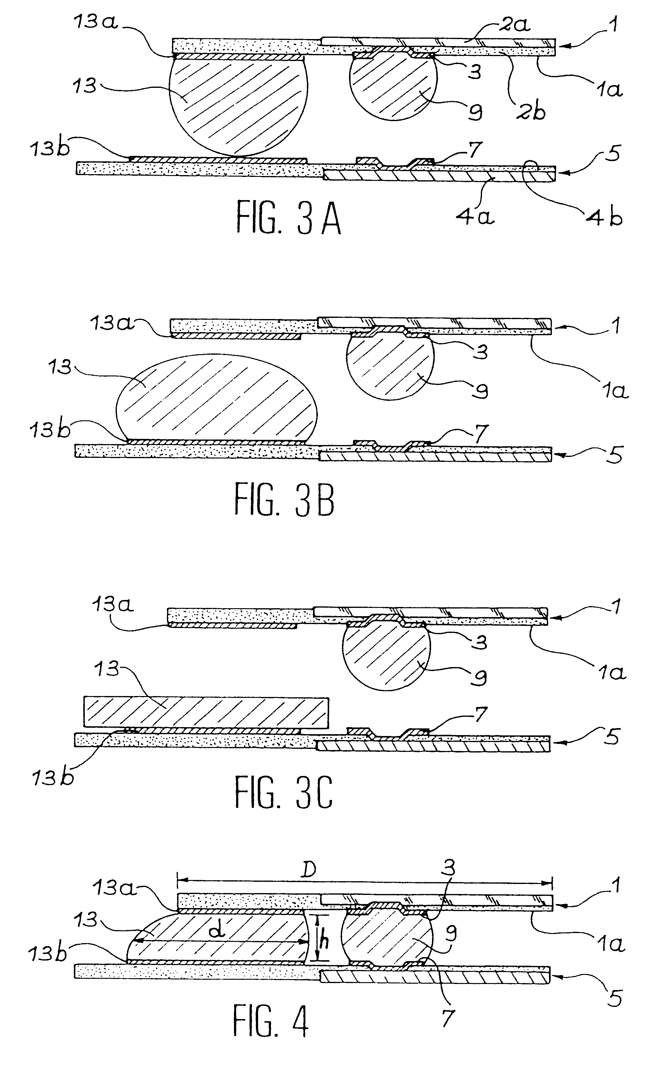
The present invention aims at obviating the disadvantages referred to hereinbefore. To this end it proposes a process for producing a ring ensuring the sealing of the chip hybridized by bumps on the substrate, whilst improving the mechanical resistance to temperature variations of the assembly constituted by the chip, the substrate and the hybridization bumps, particularly when the substrate is made from a material other than silicon.
For reasons of simplicity, said mechanical strength and sealing ring is referred to as the second material ring or even ring.
More specifically, the invention relates to a process for producing a sealing and mechanical strength ring between an interconnection substrate and an electronic component hybridized by bumps on said substrate.
This process is characterized in that it consists, parallel to the production of the hybridization bumps on a lower face of the electronic component or substrate by a first meltable material:
(a) depositing on the interconnec...
PUM
| Property | Measurement | Unit |
|---|---|---|
| Temperature | aaaaa | aaaaa |
| Mechanical strength | aaaaa | aaaaa |
| Shape | aaaaa | aaaaa |
Abstract
Description
Claims
Application Information