Printed wiring board having highly reliably via hole and process for forming via hole

a printing board and highly reliable technology, applied in the direction of resistive material coating, cable/conductor manufacturing, metallic material coating process, etc., can solve the problems of poor reliability in conduction, failure in function, and difficulty in discontinuing the via hole in the middle, so as to improve productivity, high reliability, and processing rate remarkable high

Inactive Publication Date: 2001-08-28
MITSUBISHI GAS CHEM CO INC
View PDF14 Cites 138 Cited by
  • Summary
  • Abstract
  • Description
  • Claims
  • Application Information

AI Technical Summary

Benefits of technology

The printed wiring board of the present invention and a micro-via hole formed by the method of the present invention require no desmear treatment and have high reliability with regard to connection between an outermost layer and a copper foil positioned below it. Further, the processing rate is remarkably high as compared with processing with a drill, which improves productivity to a great extent. According to the present invention, further, copper foils are etched in a thickness direction to some extent, whereby a burr occurring in a micro-via hole portion can be concurrently removed. In forming a circuit on the copper foil obtained by metal plating on each surface, therefore, defects such as a short circuit and a pattern breakage do not take place, and a high-density printed wiring board can be produced. There can be also provided a method of making a micro-via hole which makes it possible to provide the above printed wiring board.
The present invention will be explained more specifically with reference to Examples hereinafter, in which "part" stands for "part by weight" unless otherwise specified.

Problems solved by technology

When a mechanical drill is used, it is difficult to make a via hole discontinued in a middle of an intended inner-layer copper foil in its thickness direction if the inner-layer copper foil has a small thickness or if a multi-layered board varies in thickness.
In some cases, the via hole goes through the intended inner-layer copper foil and reaches a copper foil layer below the inner-layer copper foil, which causes a failure in function.
When a micro-via hole has a small diameter or when the desmear treatment is insufficient due to insufficient contact of a desmearing liquid to inner surfaces of a micro-via hole, the adhesion of a copper plating to a micro-via hole bottom is defective, which results in poor reliability in conduction.
That is, a conduction failure often takes place since the conduction between a surface-layer copper foil and a copper foil in a bottom or a wall surface of a micro-via hole is poor.
Moreover, there is another problem that the above desmear treatment requires a time period 2 to 3 times the time period of desmear treatment for a general through hole, which causes poor workability.
When a hole having a small diameter of 100 .mu.m or less is made in a copper foil by etching, there is caused a problem that the hole has poor diameter accuracy if the copper foil has a large thickness.
Furthermore, when a copper foil is present as an inner layer, even if a hole is made in a surface-layer copper foil with low energy after the concerned portion of the surface-layer copper foil is removed by etching, no hole can be made in the inner-layer copper foil, or the intended micro-via hole having a copper layer on its wall surface cannot be formed.
When a micro-via hole portion has a burr, it is required to carry out the polishing several times, which may result in a change in dimensions of the board.
Since, however, its curing rate is low and is therefore poor in workability and economic performances, etc., a known heat-curing catalyst is incorporated into the thermosetting resin.
A composition containing Na, K or Cl ion is not preferred since it has an adverse effect on the reliability of a semiconductor.
The method of preparing composition containing a metal compound powder, a carbon powder or a metal powder and an organic material is rot critical.
However, a resin adheres to vicinities of a micro-via hole in some cases during the irradiation with a carbon dioxide gas laser, and not water but an organic solvent is required for removing the above resin, which makes the processing complicated and causes problems of pollution, and the like in a post step.
It is therefore undesirable to use a resin composition soluble in an organic solvent.

Method used


Image

  • Printed wiring board having highly reliably via hole and process for forming via hole
  • Printed wiring board having highly reliably via hole and process for forming via hole
  • Printed wiring board having highly reliably via hole and process for forming via hole

Examples


example 1

900 Parts of 2,2-bis(4-cyanatophenyl)propane and 100 parts of bis(4-maleimidephenyl)methane were melted at 150.degree. C. and allowed to react with stirring for 4 hours, to obtain a prepolymer. The prepolymer was dissolved in mixed solvents of methyl ethyl ketone and dimethylformamide. To the resultant solution were added 400 parts of a bisphenol A type epoxy resin (trade name: Epikote 1001, supplied by Yuka Shell Epoxy K.K.) and a cresol novolak type epoxy resin (trade name: ESCN-220F, supplied by Sumitomo Chemical Co., Ltd.), and these materials were homogeneously dissolved and mixed. Further, as a catalyst, 0.4 part of zinc octylate was added, and these materials were dissolved and mixed. To the resultant mixture were added 500 parts of an inorganic insulating filler (trade name: baked talc, average particle diameter 0.4 .mu.m, supplied by Nippon Talc K.K.) and 8 parts of a black pigment, and these materials were homogeneously stirred and mixed to prepare a varnish A. A 100 .mu.m...

example 2

1,400 Parts of an epoxy resin (trade name: Epikote 5045), 600 parts of an epoxy resin (trade name: ESCN220F), 70 parts of dicyandiamide and 2 parts of 2-ethyl-4-methylimidazole were dissolved in mixed solvents of methyl ethyl ketone and dimethyformamide. Further, 500 parts of the same insulating inorganic filler as that in Example 1 was added, and the mixture was forcibly stirred to form a homogeneous dispersion, whereby a varnish D was obtained. A 50 .mu.m thick glass woven fabric was impregnated with the varnish D and the impregnated glass woven fabric was dried to give a prepreg (prepreg E) having a gelation time of 150 seconds and having a glass cloth content of 35% by weight. One sheet of the prepreg E was used, and a 18 .mu.m thick electrolytic copper foil was placed on each surface, and the resultant set was laminate-formed at 190.degree. C. at 20 kgf / cm.sup.2 under a vacuum of 30 mmHg or less for 2 hours, to prepare a double-side copper-clad laminate F. The insulating layer ...

example 3

A sheet with a film having a copper oxide powder content of 20% by volume and having a melting point of 83.degree. C. was prepared in the same manner as in Example 1 except that the 50 .mu.m thick polyethylene terephthalate film used in Example 1 was replaced with a 25 .mu.m thick polyethylene terephthalate film.

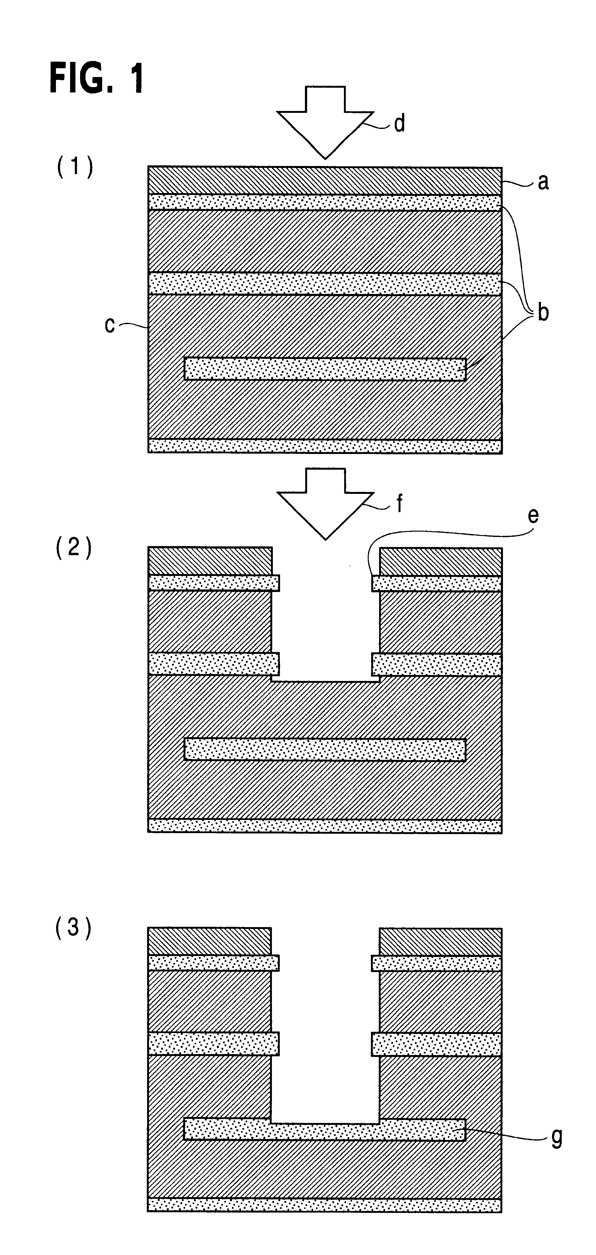
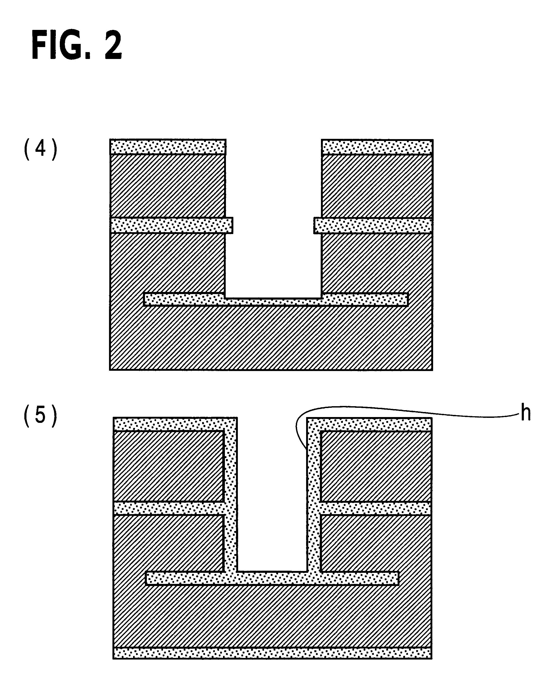
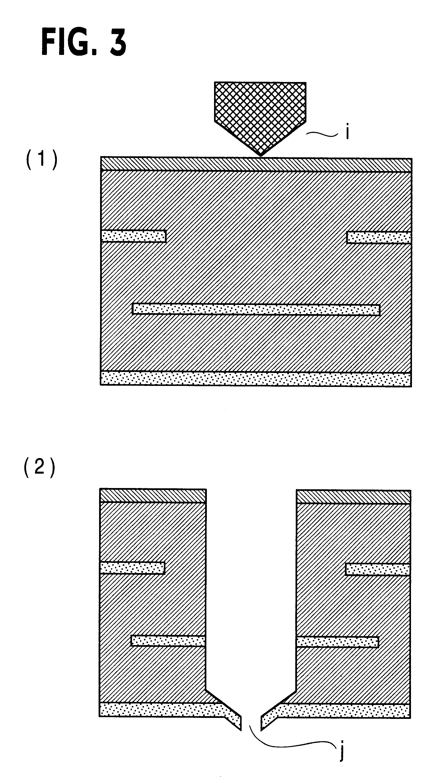
The above sheet was laminated on the same double-side copper-clad laminate B as that obtained in Example 1 at 90.degree. C., and the sheet was 2 shots irradiated with a carbon dioxide gas laser at an output of 40 mJ / pulse, to make 900 holes having a diameter of 100 .mu.m each at intervals of 400 .mu.m. Then, an copper foil as an inner layer was 1 shot irradiated with the carbon dioxide gas laser at a decreased output of 7 mJ / pulse to remove surface portions of the copper foil in portions which were to form micro-via hole bottoms. In this manner, micro-via holes were made in 70 blocks (63,000 micro-via holes as a total). Then, the front and reverse surfaces of the board were ...


PUM

PropertyMeasurementUnit
thicknessaaaaaaaaaa
bond energyaaaaaaaaaa
melting pointaaaaaaaaaa

Abstract

Disclosed are a printed wiring board having micro-via holes highly reliable for conduction and a method of making the micro-via hole by providing a coating or sheet of an organic substance containing 3 to 97% by volume of at least one selected from a metal compound powder, a carbon powder or a metal powder having a melting point of at least 900° C. and a bond energy of at least 300 kJ/mol on a copper foil as an outermost layer of a copper-clad laminate having at least two copper layers, or providing a coating or sheet of the same after oxidizing a copper foil as an outermost layer, irradiating the coating or sheet with a carbon dioxide gas laser at an output of 20 to 60 mJ/pulse, thereby removing a micro-via-hole-forming portion of at least the copper foil as the outermost layer, then irradiating micro-via-hole-forming portions of the remaining layers with a carbon dioxide gas laser at an output of 5 to 35 mJ/pulse to make a micro-via hole which does not penetrate through the copper foil in a bottom of the micro-via hole, and electrically connecting the copper foil as the outermost layer and the copper foil in the bottom of the micro-via hole with a metal plating or an electrically conductive coating composition.

Description

The present invention relates to a printed wiring board having a micro-via hole. More specifically, it relates to a printed wiring board having a structure in which a micro-via hole is formed by removing part of surface of a copper foil positioned below an outermost layer, i.e., a surface layer, so as not to penetrate through the copper foil in the bottom, and the surface layer and the copper foil are electrically connected with a plating or an electrically conductive coating composition forming a wall surface of the micro-via hole, the printed wiring board being highly reliable with regard to conduction and being mainly for use for a small-sized semiconductor plastic package.PRIOR ART OF THE INVENTIONIn a high-density multi-layered printed wiring board for use in a semiconductor plastic package, conventionally, a via hole is made directly with a mechanical drill, or it is made by removing a hole-forming portion of a surface-layer copper foil by etching and then making a hole in an ...

Claims


Application Information

Patent Timeline
Patent Type & Authority Patents(United States)
IPC IPC(8): B23K26/38B23K26/00H05K3/42H05K3/00H05K3/38
CPCB23K26/385H05K3/0038H05K3/429H05K3/0035Y10T29/49155H05K3/0055H05K3/385H05K2201/0112H05K2201/0215H05K2201/0323H05K2201/09518H05K2201/0969H05K2203/0315H05K2203/095H05K2203/1383Y10T29/49165B23K26/389H05K3/42
Inventor GAKU, MORIOIKEGUCHI, NOBUYUKITANAKA, YASUO
Owner MITSUBISHI GAS CHEM CO INC
Why Eureka
Try Eureka