
Apparatus and method for plasma etching

Inactive Publication Date: 2001-05-29
PANASONIC CORP
View PDF5 Cites 39 Cited by
  • Summary
  • Abstract
  • Description
  • Claims
  • Application Information

AI Technical Summary

Benefits of technology

According to the present invention, therefore, the etching conditions can be set so that the product of the distance between the parallel plate electrodes and the pressure of the mixed gas in the treatment chamber takes a value within a predetermined range respectively for improving the etching efficiency. The plasma etching can thus be conducted at a lower cost and more efficiently.

Problems solved by technology

However, such a conventional plasma etching has been confronted with the following problems.
Therefore, if the surface must be removed more, the etching treatment takes a long time and further, since a high vacuum degree is required, the exhaust process for evacuation takes a long time for each treatment cycle.
Along with such a low etching rate described above, those long time treatments result in further significant reduction of the efficiency in the entire substrate treatment.
Furthermore, because the conventional plasma etching requires such a high vacuum degree, the cost of the vacuum system facility also rises significantly.
And furthermore, because the object substrate is placed in such a high vacuum state, it is impossible to employ a method of vacuum suction to hold the substrate.
Instead, an expensive electrostatic suction method or a mechanical holding method had to be employed to hold the substrate.
This was why it was very difficult to simplify the facility and reduce the cost of the facility.
In addition, in case of the conventional plasma etching, it was difficult to generate the plasma in uniform between the electrodes.
Thus, the etching effect was partially varied on the object substrate, which made stable etching difficult.
Accordingly, in such the conventional plasma etching, there was a problem that it was difficult to process the etching for the substrate at a low cost, in uniform, and efficiently.

Method used


Image

  • Apparatus and method for plasma etching
  • Apparatus and method for plasma etching
  • Apparatus and method for plasma etching

Examples


Embodiment Construction

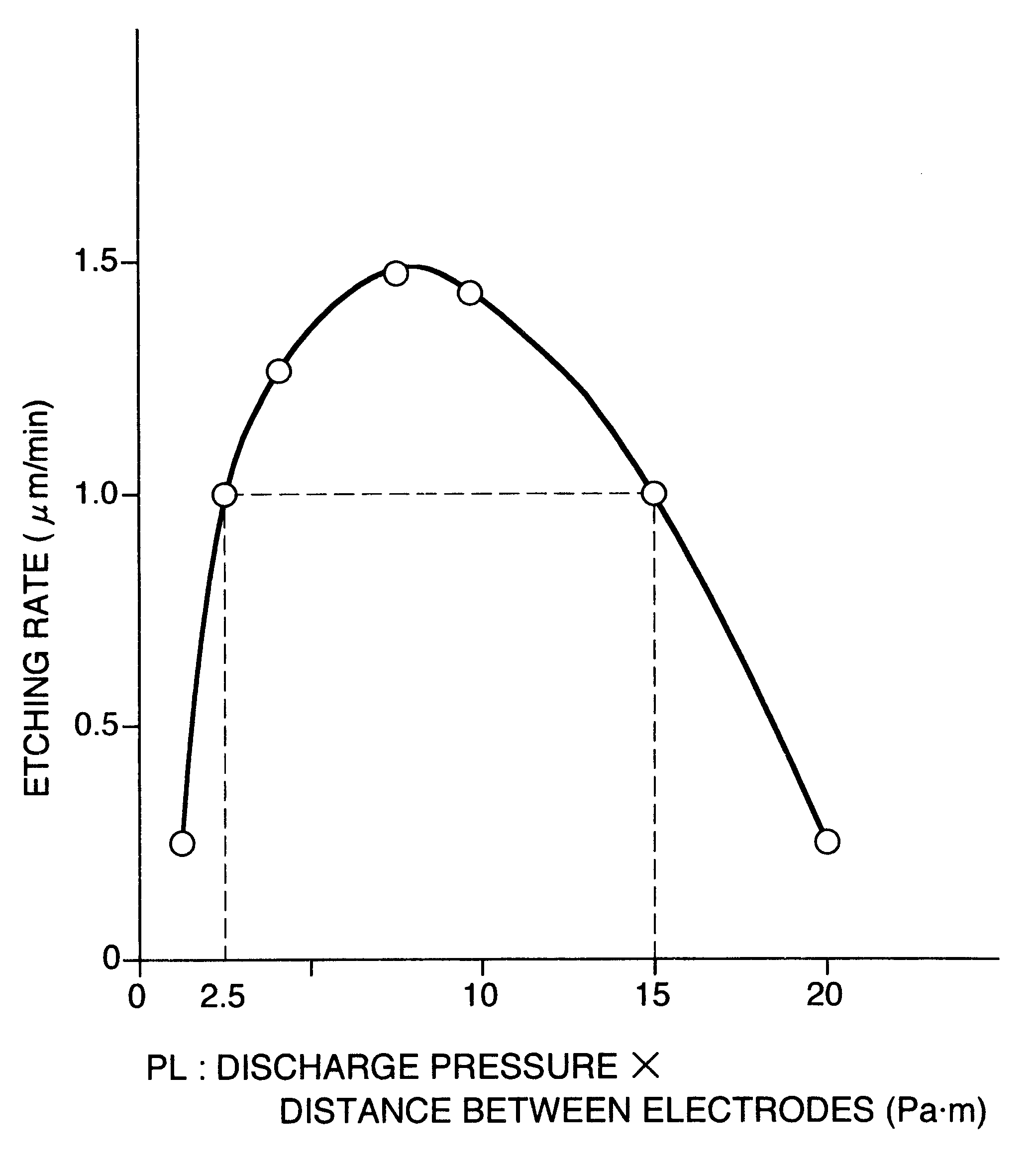
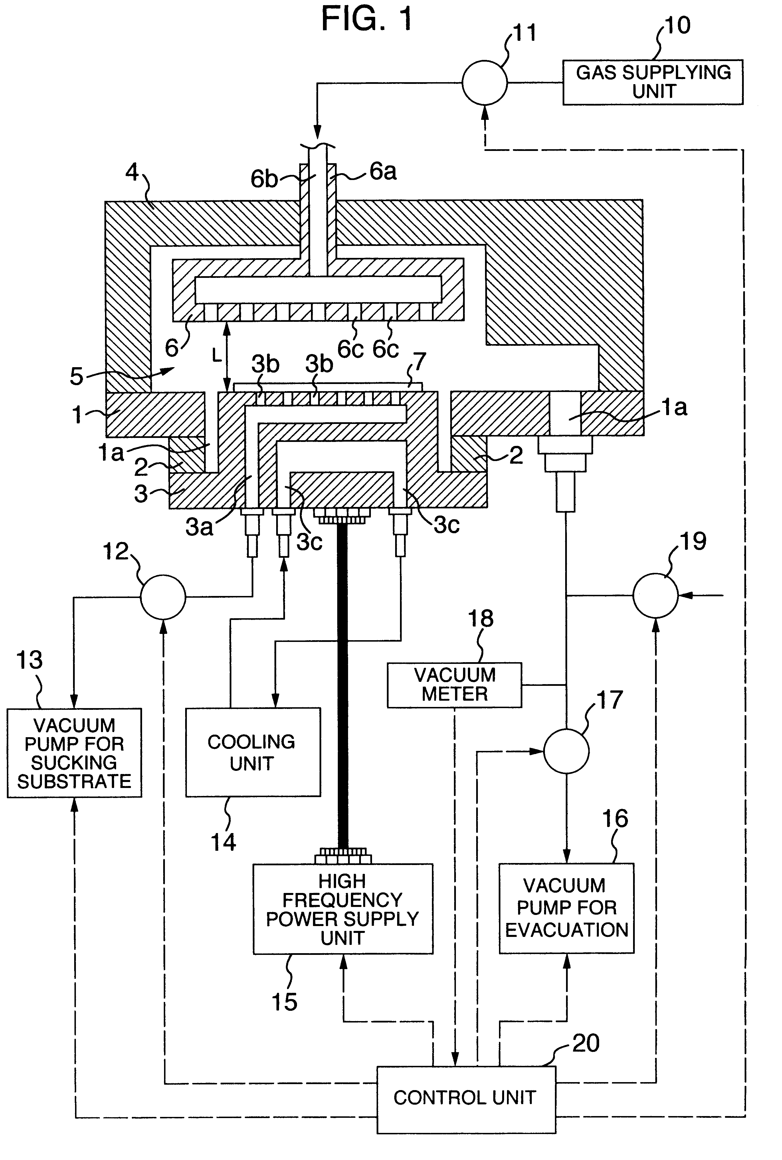
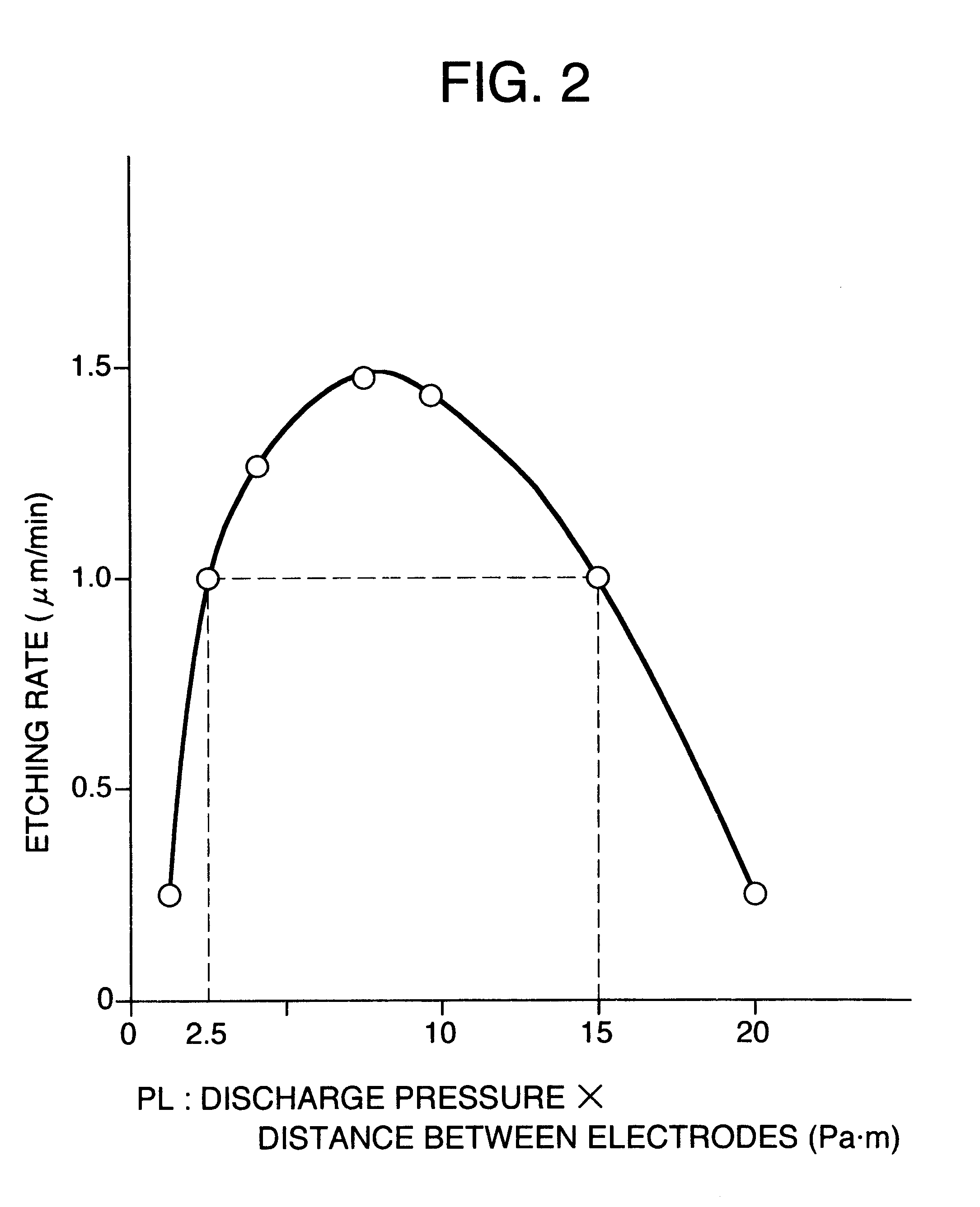
FIG. 1 is a cross sectional view of a plasma etching apparatus in a first embodiment according to the present invention. FIG. 2 is a graph showing an etching rate of the same plasma etching apparatus. FIG. 3 is a graph showing a plasma etching condition of the same. FIGS. 4A to 4E show the processes of manufacturing the semiconductor device in the first embodiment.

At first, the plasma etching apparatus will be described with reference to FIG. 1. In FIG. 1, a base member 1 is provided with an aperture 1a. A lower electrode assembly 3 is fit in the aperture 1a via an insulating member 2 from the bottom side. A covering member 4 is put on the base member 1 air-tightly. A space enclosed tightly by the covering member 4, the lower electrode assembly 3 and the base member 1 is used as a treatment chamber 5 for performing plasma etching for an object substrate 7 to be treated placed on the lower electrode assembly 3. The covering member 4 is moved up / down by an up / down moving member (not i...


PUM

PropertyMeasurementUnit
Fractionaaaaaaaaaa
Fractionaaaaaaaaaa
Pressureaaaaaaaaaa

Abstract

A plasma etching apparatus and a plasma etching method for conducting a plasma etching treatment for a substrate to be treated placed on one of parallel plate electrodes disposed oppositely to each other in a treatment chamber, wherein gas supplying device is used to supply a mixed gas including oxygen and a fluorine gas in the treatment chamber and the plasma discharge is conducted between the parallel plate electrodes under the condition that the product PL of a distance L[m] between the plate electrodes and the pressure P[Pa] of the mixed gas in the treatment chamber takes a value within 2.5[Pa.m] to 15[Pa.m] so as to efficiently perform an etching treatment, at a low cost, and in uniform.

Description

The present invention relates to an apparatus and a method for plasma etching processing silicon substrates applied to semiconductor devices or the like.RELATED ARTPlasma etching is a well-known method for treating silicon substrates applied to semiconductor devices or the like. According to this method, an object to be treated, for example, a silicon substrate is treated as follows. At first, the silicon substrate is placed in a treatment chamber, which is then evacuated. After evacuation, a gas for generating plasma is supplied in the chamber, then a high frequency voltage is applied to between electrodes disposed therein so as to generate plasma. As a result, ions and electrons are generated in the chamber and the substrate is treated by the etching action of those ions and electrons. Conventionally, those electrodes for discharging the plasma were disposed so as to be separated by approximately 30 to 80 mm from each other and the pressure in the treatment chamber was lowered up ...

Claims


Application Information

Patent Timeline
IPC IPC(8): H01L21/02H01L21/3065H01L21/00H01L21/302C23F4/00H01L21/78H05H1/46
CPCH01J37/32082H01L21/3065H01L21/78H01L21/67069
Inventor ARITA, KIYOSHIHAJI, HIROSHI
Owner PANASONIC CORP
Learn More