Method for reducing dark current effects in a charge couple device

a charge couple device and charge current technology, applied in the field of charge current reduction, can solve the problems of excessive dark current destroying the dynamic range of the ccd array, dark current defects, and particularly perplexing problems of the charge couple device, so as to reduce the leakage from pixel to pixel, reduce the effect of dark current effects, and permit the absorption of sufficient ligh

Inactive Publication Date: 2001-08-07
IBM CORP
View PDF8 Cites 66 Cited by
  • Summary
  • Abstract
  • Description
  • Claims
  • Application Information

AI Technical Summary

Benefits of technology

The present invention overcomes problems of the prior art and provides for trapping hydrogen on the surface of the cell to minimize leakage from pixel to pixel and still permit the absorption of sufficient light. The present invention provides for at least significantly reducing the dark current effects in a charge couple device. In fact, the present invention makes it possible to achieve active storage area dark currents of less than 250 picoamps / cm.sup.2 on full frame, progressive scan CCD image sensors incorporating vertical anti-blooming device structures.

Problems solved by technology

A particularly perplexing problem of charge couple devices is referred to as dark current.
Excessive dark current destroys the dynamic range of the CCD array when there is insufficient ability to distinguish between light and dark conditions.
The problem concerning dark current defects is especially critical in consumer digital still picture applications where cameras must function in both bright (short shutter speed) and low (long shutter speed) light conditions.
However, while hydrogen could be used to solve the problem, keeping the hydrogen in the device is problematic since hydrogen diffuses very readily.
PECVD films are too high in stress with the addition of sufficient hydrogen.
In addition, an attempt with a relatively thick (e.g. 1750 angstroms) hydrogen enriched PECVD reduced dark current, but the thickness of the film actually destroyed the necessary light transmissivity of the array.
On the other hand, use of a relatively thin (e.g. 300 angstroms) hydrogen enriched PECVD nitride film had undesirable stress characteristics but adequate light transmissivity.
Furthermore, LPCVD films by comparison are very low in hydrogen content and also create integration problems due to the long heat cycle.
Therefore, they are unable to provide a sufficient hydrogen reservoir.

Method used


Image

  • Method for reducing dark current effects in a charge couple device

Examples


Embodiment Construction

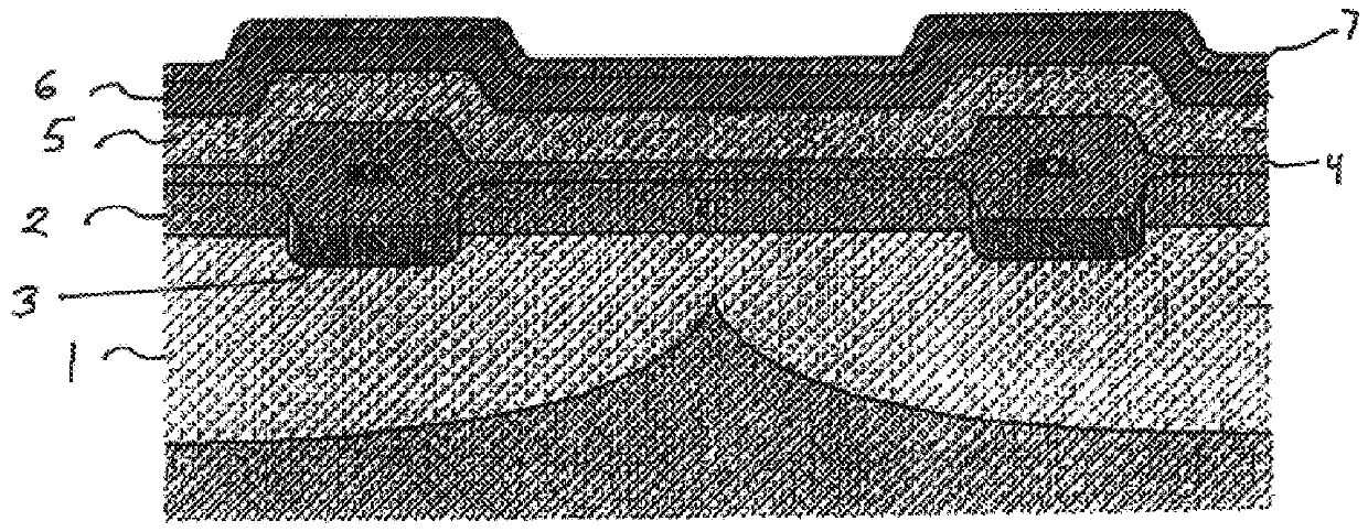
In order to facilitate an understanding of the present invention, reference will be made to the FIGURE. In particular, numeral 1 illustrates a p-well for collecting charge as present in a conventional CCD array. Numeral 2 represents a typical buried channel and 3 illustrates a typical channel stop. The thermally grown oxide 4 acts as a barrier between pixels and 5 is typically a doped polycrystalline silicon layer which functions to carry the charge generated by the light.

Also present is layer 6 which is typically an oxidized polycrystalline silicon layer. Layer 6 acts to reduce capacitance to other passing polycrystalline silicon layers. The layers 1-6 and methods for their fabrication are well known in the art and need not be described in any further detail herein.

According to the present invention, a hydrogen-enriched silicon nitride film 7 is deposited on top of barrier layer 6. Prior to depositing the nitride film 7 the charge couple device is subjected to an anneal in hydrogen...


PUM

PropertyMeasurementUnit
temperatureaaaaaaaaaa
pressureaaaaaaaaaa
thicknessaaaaaaaaaa

Abstract

The dark current defects in a charge couple device are reduced by employing a hydrogen anneal followed by depositing a silicon nitride barrier layer by RTCVD.

Description

The present invention relates to a method for significantly reducing, if not eliminating, the dark current effects in a charge couple device (CCD). More particularly, the present invention involves a combination of a hydrogen anneal followed by depositing a hydrogen-rich barrier layer of silicon nitride by rapid thermal chemical vapor deposition (RTCVD). In addition, the present invention relates to charge couple devices obtained according to the process of the present invention. The process of the present invention makes it possible to achieve active storage area dark currents of less than 250 picoamps / cm.sup.2 on full frame, progressive scan CCD image sensors incorporating vertical anti-blooming device structures.BACKGROUND OF INVENTIONA charge couple device (CCD) functions as an active matrix to absorb light and convert it to electrons. Such are used for example as the electronic film in digital still cameras(DSC).Desirably, a charge couple device should absorb as much light as p...

Claims


Application Information

Patent Timeline
Patent Type & Authority Patents(United States)
IPC IPC(8): H01L27/148
CPCH01L27/14887H01L27/14812
Inventor BALLANTINE, ARNE W.DUNBAR, III, GEORGE A.HART, III, JAMES V.JOHNSON, DONNA K.MACDOUGALL, GLENN C.
Owner IBM CORP
Why Eureka
Try Eureka