Provably correct storage arrays

a technology of provably correct arrays and arrays, applied in the direction of software simulation/interpretation/emulation, program control, instruments, etc., can solve the problems of limiting the possible implementation of styles, and affecting the design effect of arrays

Inactive Publication Date: 2001-08-21
IBM CORP
View PDF4 Cites 19 Cited by
  • Summary
  • Abstract
  • Description
  • Claims
  • Application Information

AI Technical Summary

Problems solved by technology

As the number of transistors used for complex logic and memory increases on a central processing unit (CPU) chip, the verification of intended functionality versus the actual functionality becomes a major task.
The automation may limit the possible implementation of styles as it can grab fixed cells from the designated libraries.
This may not result in optimization of area, timing and power.
However, many times these limit the performance.
The smaller granularity of this model causes a significant increase in simulation complexity.
This reduces total number of patterns which in turn reduce the verification coverage.
In spite of these developments these repeated functional simulations on the circuit level is highly time-intensive and difficult for user friendly applications.
Even though the specification is listed "fully functional", at the transistor level design may result in errors due to limitations on the test pattern coverages.
The verification of a memory unit is done by partitioning logic and array on the chip, since the verificati

Method used


Image

  • Provably correct storage arrays
  • Provably correct storage arrays
  • Provably correct storage arrays

Examples


Embodiment Construction

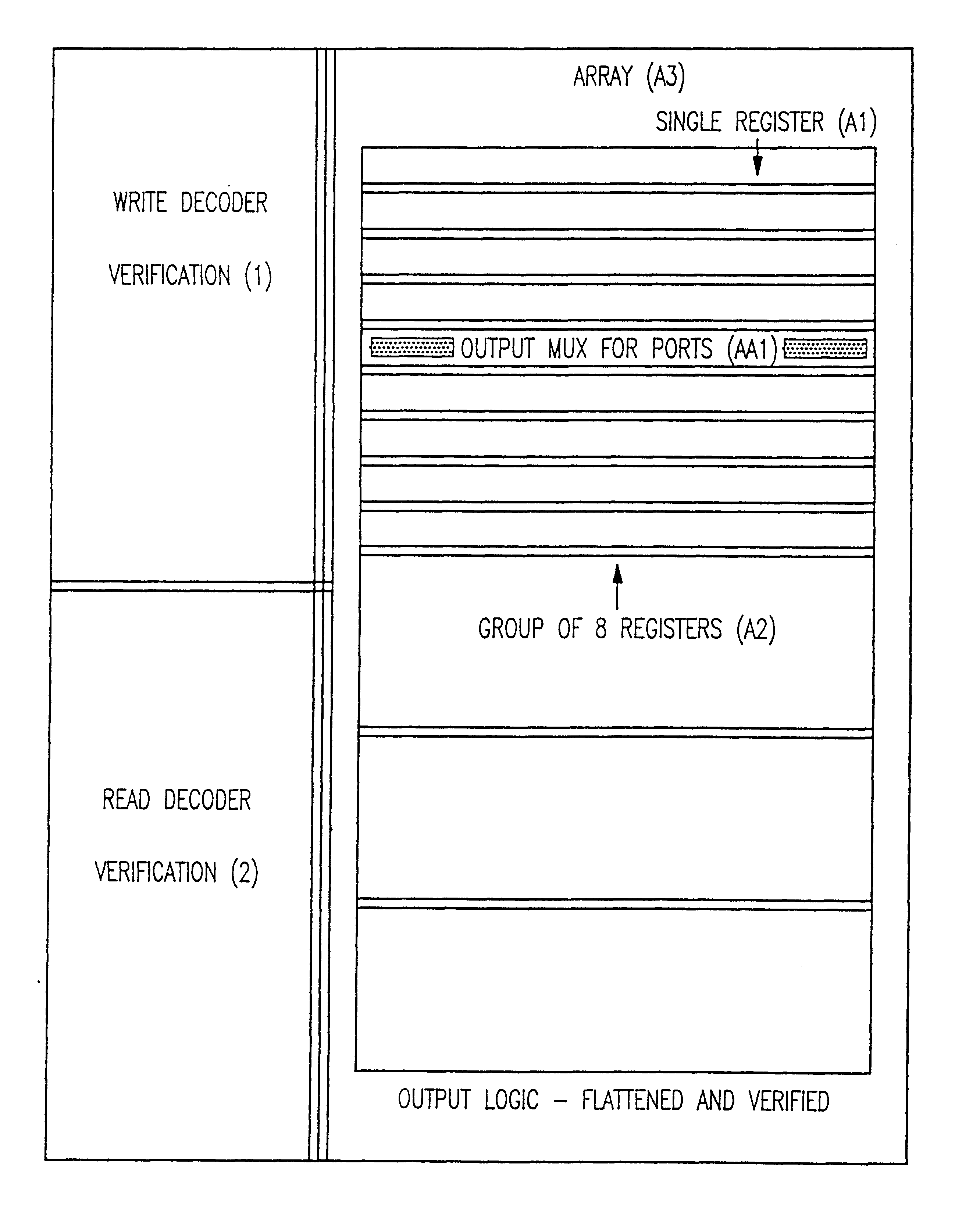
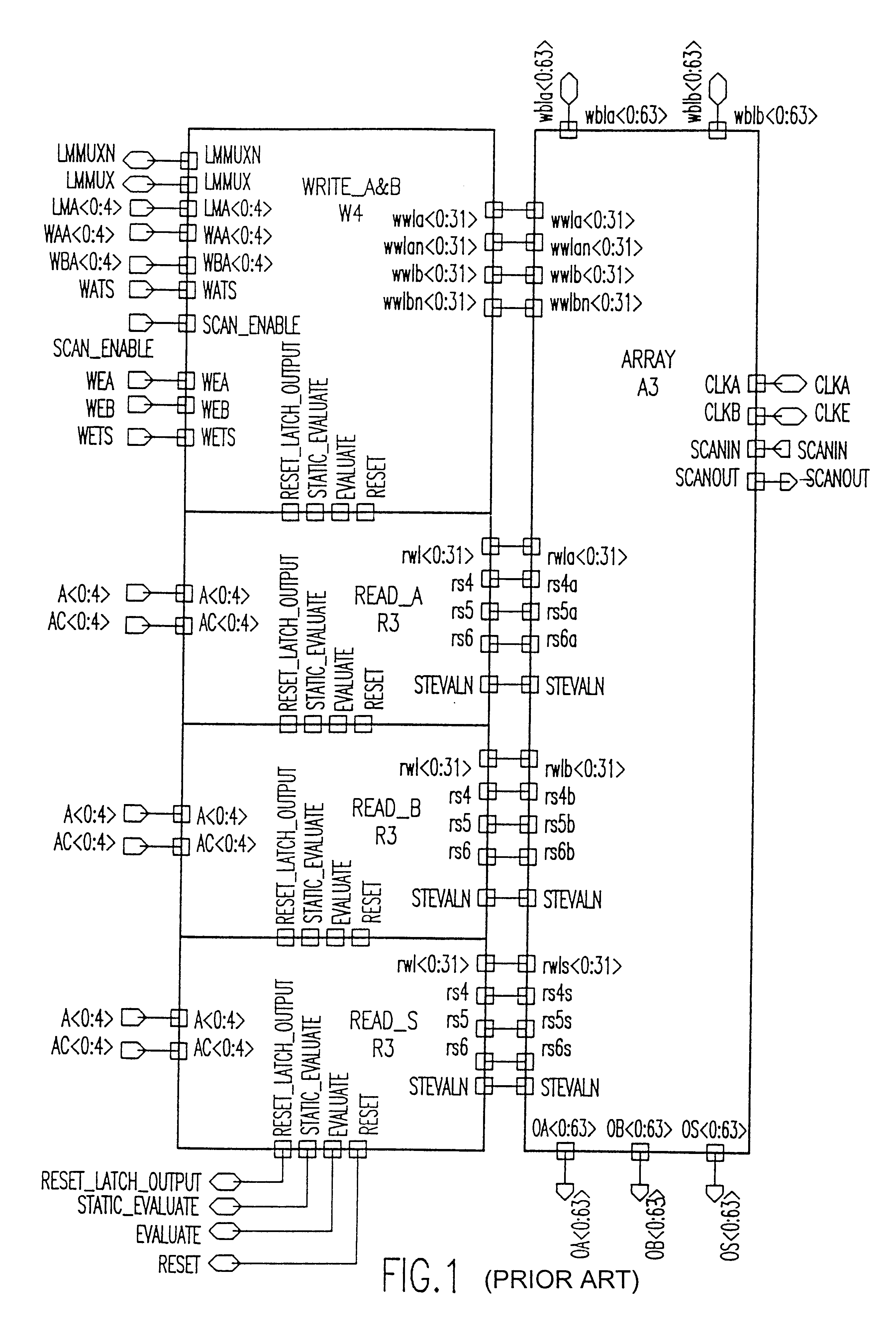
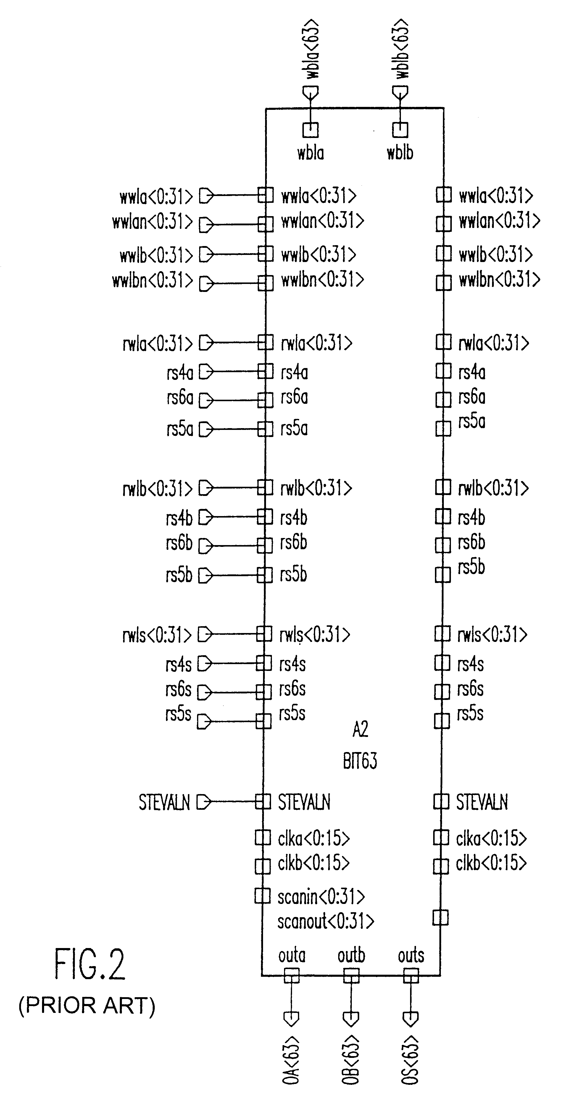
The process for verification is based on Boolean Extraction of the macro based on various algorithms. Such an extraction is compared with the logic representation. For memory and logic macros, the extraction is tightly coupled with the actual verification step. This makes it possible to efficiently handle special structures such as pass-transistor logic, false CMOS paths or circuits which contain combinatorial loops. This particular methodology checks dynamic circuits and nets which would potentially violate the combinatorial verification model. Also, the verification method for memory circuit is fully customized by user defined extraction rules, such as, for example, the dual rail signal inputs, elimination of resetting paths or precharge paths, black boxing unwanted elements etc. The rule set also includes tests for unwanted circuit situations such as nets which might have floating states.

Logic and Memory Circuit Verification

FIG. 1 shows an example of a memory circuit along with p...


PUM


Abstract

A hardware design technique allows checking of design system language (DSL) specification of an element and schematics of large macros with embedded arrays and registers. The hardware organization reduces CPU time for logical verification by exponential order of magnitude without blowing up a verification process or logic simulation. The hardware organization consists of horizontal word level rather than bit level. A memory array cell comprises a pair of cross-coupled inverters forming a first latch for storing data. The first latch has an output connected to a read bit line. True and complement write word and bit line input to the first latch. A first set of pass gates connects between the true and complement write word and bit line inputs via gates and the input of said first latch. The first set of pass gates is responsive to a first clock via a second pass gate. A pair of cross-coupled inverters forms a second latch of a Level Sensitive Scan Design (LSSD). The second latch has output connected to an LSSD output for design verification. A second pass gate connects between the output of the first set of pass gates and the input of said first latch. The second pass gate is responsive to said first clock. A third pass gate connects between the output of said first latch and the input of said second latch. The third pass gate is responsive to a second clock. The first and second clocks are responsive to a black boxing process for incremental verification.

Description

1. Field of the InventionThe present invention generally relates to design of provably correct arrays in complex logic and memory systems implemented in very large scale integrated (VLSI) circuits and, more particularly, to a hardware design technique that allows checking the design system language (DSL) specification of large macros with embedded arrays and registers.2. Background DescriptionAs the number of transistors used for complex logic and memory increases on a central processing unit (CPU) chip, the verification of intended functionality versus the actual functionality becomes a major task. To illustrate this point, many top level circuits as well individual circuits need to be evaluated with respect to static function, timing, testability of scan chain and manufacturability. As a result, a complete verification of logic and memory on a CPU chip is a necessity for low development cost and short design delivery cycles.In the verification process, user-defined functions are c...

Claims


Application Information

Patent Timeline
IPC IPC(8): G01R31/28G01R31/3185
CPCG01R31/318536Y10S257/903
Inventor HENKELS, WALTER HARVEYHWANG, WEIJOSHI, RAJIV VASANTWILLIAMS, ALBERT THOMAS
Owner IBM CORP
Why Eureka
Try Eureka