Method of recycling a delaminated wafer and a silicon wafer used for the recycling

a technology of delaminated wafers and recycling methods, which is applied in the direction of basic electric elements, electrical apparatus, semiconductor devices, etc., can solve the problems of large portion of one of the wafers being pulverized and lost, and the method ofsimox has many

Inactive Publication Date: 2001-09-04
SHIN-ETSU HANDOTAI CO LTD
View PDF12 Cites 108 Cited by
  • Summary
  • Abstract
  • Description
  • Claims
  • Application Information

AI Technical Summary

Problems solved by technology

However, the SIMOX method has many problems in relation to the reliability of a buried oxide layer, the crystallinity of the SOI layer, necessity of heat treatment at a temperature of 1300.degree. C. or higher, and the like.
However, since the thin film is formed by means of mechanical machining, it takes long time to form the thin film, and a great portion of one of the wafers is pulverized to be lost.
Therefore, productivity is extremely low, and production cost is significantly high.
Furthermore, there are limits to the thickness and thickness uniformity of the resultant SOI layer in formation of the thin film by grinding and polishing by means of mechanical machining.
However, it has been found in recent years that there exist in the CZ wafer crystal defects called COP (Crystal Originated Particle) which are incorporated while the crystal is growing.
However, since it is necessary to use an expensive epitaxial wafer, production cost of the SOI wafer gets far higher.
However, since only one SOI wafer can be obtained from two silicon wafers, there still exists the problem of high production cost.
It is conceptually possible to reuse the delaminated wafer, but there has been no actual cases of reusing the delaminated wafer, and the specific means for reusing it has not yet been known.
However, in order to improve the surface properties by grinding and polishing, long processing time and a lot of stock removal are required.
Moreover, in the case that an epitaxial layer is used as a bond wafer in the hydrogen ion delimitation method, and SOI layer is made of an epitaxial layer, since the epitaxial layer remaining on the delaminated layer is completely removed, the epitaxial layer cannot be reused as a SOI layer.
Accordingly, cost for fabrication of SOI wafer cannot be reduced.
In the case that CZ wafer is used as a bond wafer, the problems in relation to the above-mentioned COP cannot be solved by grinding and polishing.
In the case that FZ wafer is used as a bond wafer, a lot of stock removal in grinding or polishing means the small number of times of reuse, and further, long processing time, and high production cost.
Furthermore, since the oxide film and the silicon are different in hardness, uniform polishing is difficult in the presence of the oxide film.

Method used


Image

  • Method of recycling a delaminated wafer and a silicon wafer used for the recycling
  • Method of recycling a delaminated wafer and a silicon wafer used for the recycling
  • Method of recycling a delaminated wafer and a silicon wafer used for the recycling

Examples


example 1

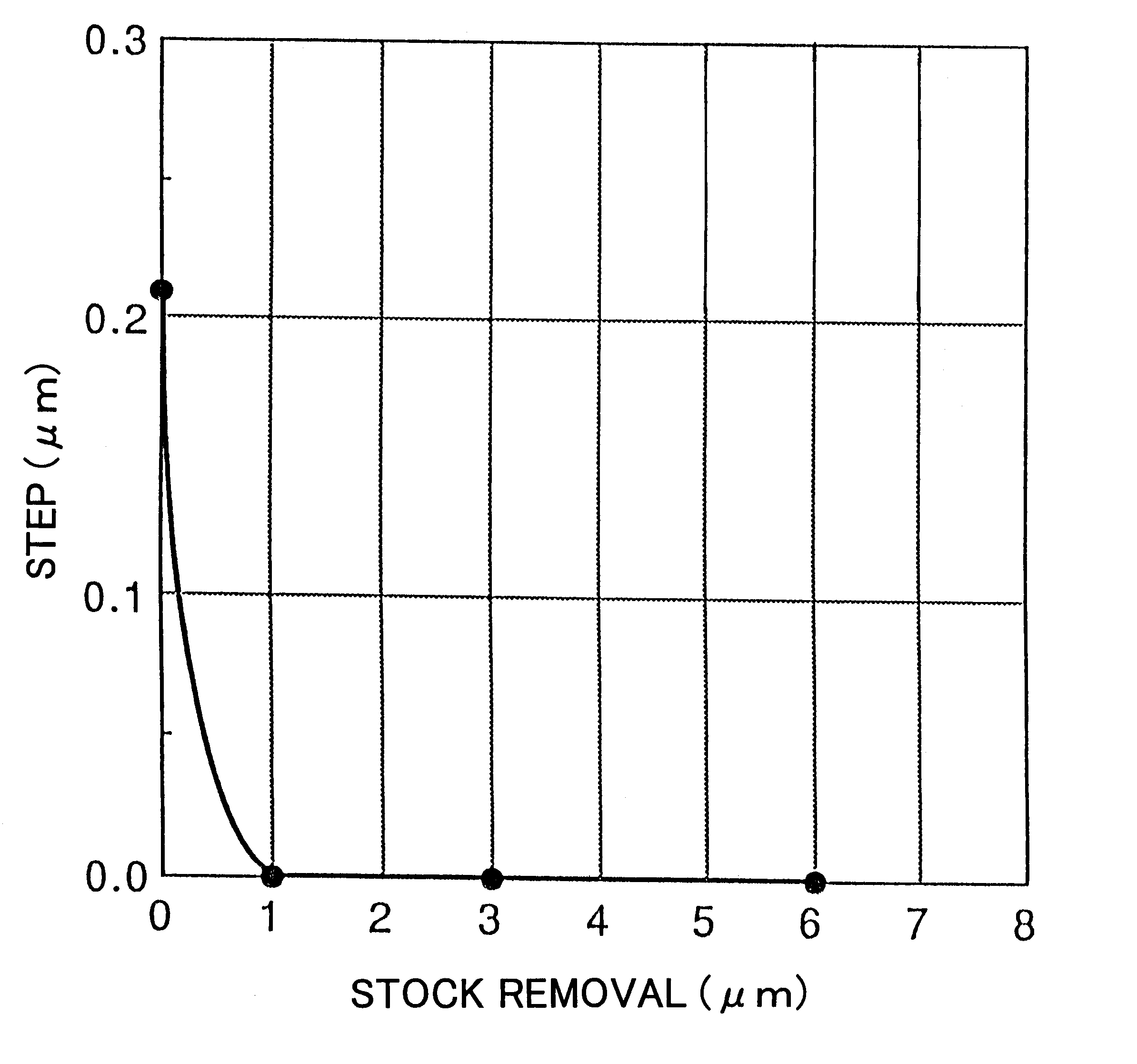
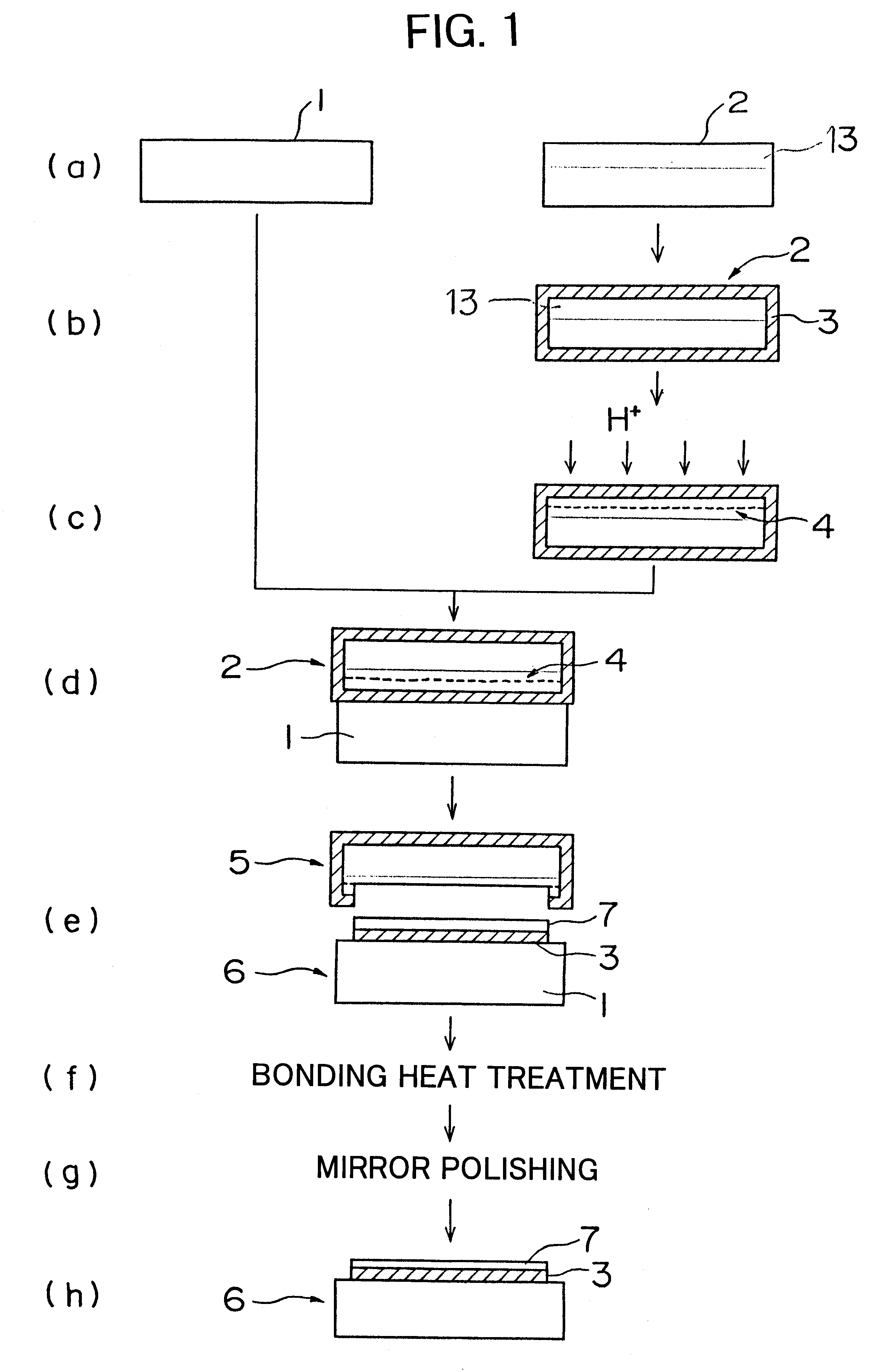
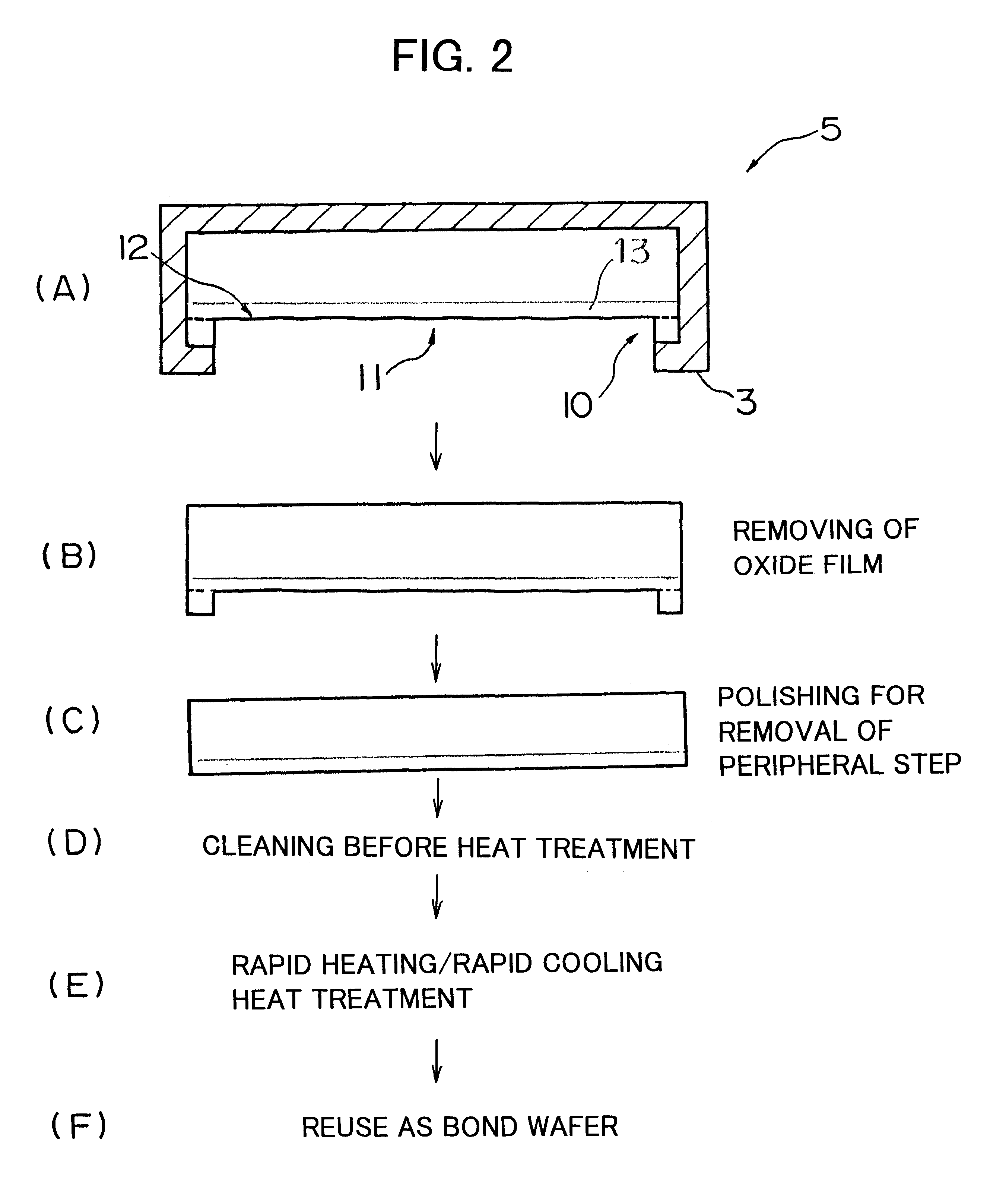
Two silicon mirror wafers having resistivity of 1.0 to 2.0 .OMEGA..multidot.cm and a diameter of 150 mm wherein a conductive type is p type were prepared. As for one of these wafers, an epitaxial layer having a thickness of about 10 microns was grown. The epitaxial wafer was used as a bond wafer, and processed through steps (a) to (h) shown in FIG. 1 according to the hydrogen ion delaminating method to fabricate SOI wafers. Thickness of SOI layer was 0.2 micron. The major process conditions used in the method were as follows.

1) Thickness of a buried oxide layer: 400 nm (0.4 micron);

2) Conditions of hydrogen implantation: H.sup.+ ions, implantation energy of 69 keV, implantation dose of 5.5.times.10.sup.16 / cm.sup.2 ;

3) Conditions of heat treatment for delamination: in a N.sub.2 gas atmosphere, at 500.degree. C. for 30 minutes.

4) Conditions of heat treatment for bonding: in a N.sub.2 gas atmosphere, at 1100.degree. C. for 2 hours.

The high quality SOI wafer having the SOI layer of the...


PUM

PropertyMeasurementUnit
melting pointaaaaaaaaaa
thicknessaaaaaaaaaa
thicknessaaaaaaaaaa

Abstract

There is disclosed a method of recycling a delaminated wafer produced as a by-product in producing an SOI wafer according to a hydrogen ion delaminating method by reprocessing it for reuse as a silicon wafer, wherein at least polishing of the delaminated wafer for removing of a step in the peripheral part of the delaminated wafer and heat treatment in a reducing atmosphere containing hydrogen are conducted as the reprocessing. There are provided a method of appropriately reprocessing a delaminated wafer produced as a by-product in a hydrogen ion delaminating method to reuse it as a silicon wafer actually, and particularly, a method of reprocessing an expensive wafer such as an epitaxial wafer many times for reuse, to improve productivity of SOI wafer having a high quality SOI layer, and to reduce producing cost.

Description

1. Field of the InventionThe present invention relates to a method of recycling a silicon wafer by reprocessing a delaminated (split) wafer produced as a by-product in a hydrogen ion delaminating method (also called a smart cut method) wherein an ion-implanted wafer is bonded to another wafer and a portion of the ion-implanted wafer is delaminated to thereby obtain an SOI (silicon on insulator) wafer. Particularly, the present invention relates to a method of reprocessing the delaminated wafer many times, and reusing it many times.2. Description of the Related ArtConventionally, two methods have gained wide notice as methods of fabricating wafers having an SOI structure. One method is a SIMOX (separation by implanted oxygen) method in which oxygen ions are implanted into a silicon monocrystal at a high concentration, and heat treatment is then performed at a high temperature in order to form an oxide layer. The other method is a bonding method in which two mirror-polished silicon wa...

Claims


Application Information

Patent Timeline
Patent Type & Authority Patents(United States)
IPC IPC(8): H01L21/762H01L21/02H01L21/20H01L21/70H01L27/12H01L21/265
CPCH01L21/02032H01L21/2007H01L21/76254Y10S438/959Y10S438/977
Inventor KUWAHARA, SUSUMUMITANI, KIYOSHIAGA, HIROJIWADA, MASAE
Owner SHIN-ETSU HANDOTAI CO LTD
Why Eureka
Try Eureka