Method of forming fluorosilicate glass (FSG) layers with moisture-resistant capability
- Summary
- Abstract
- Description
- Claims
- Application Information
AI Technical Summary
Problems solved by technology
Method used
Image
Examples
Embodiment Construction
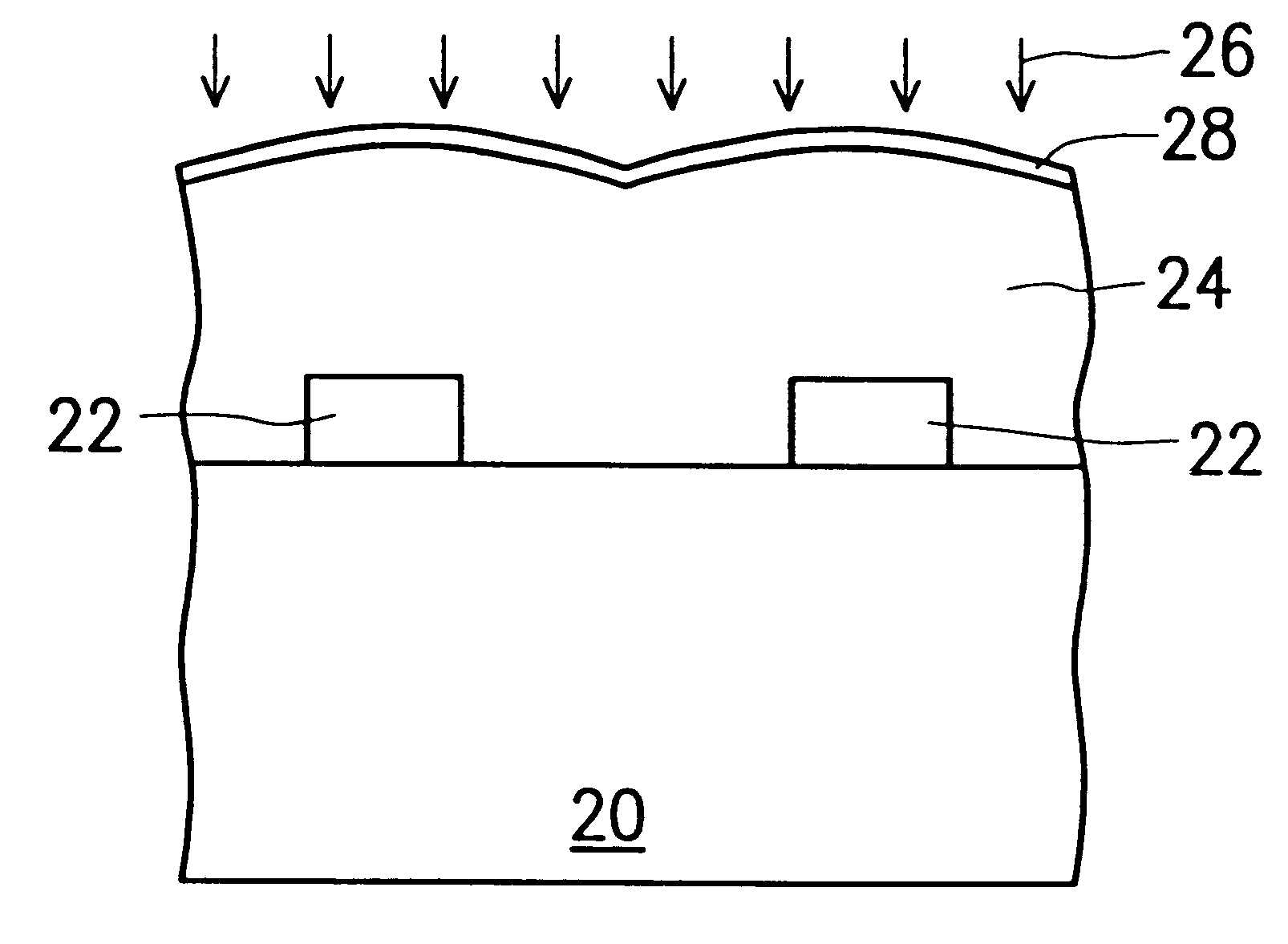
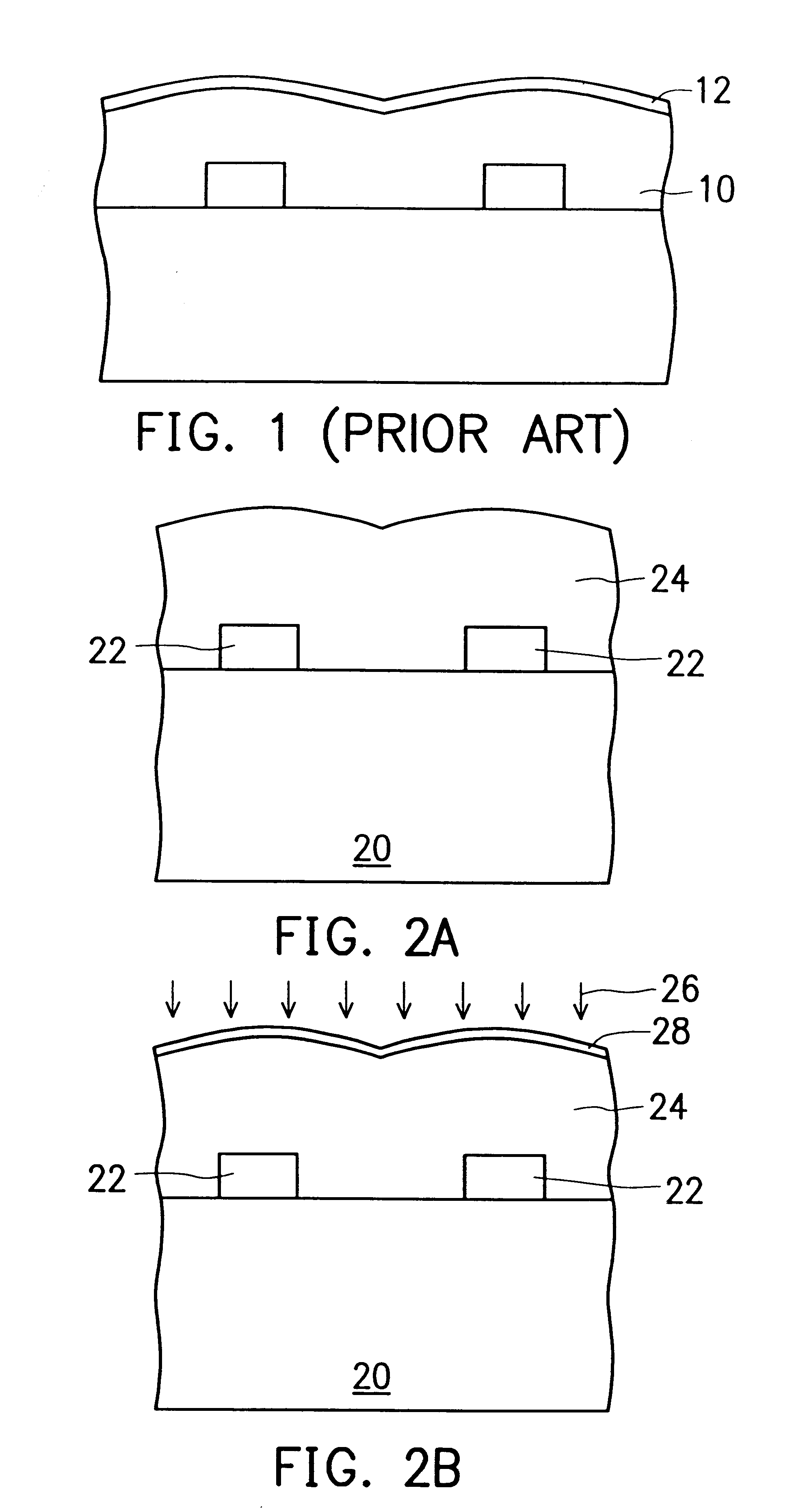
FIGS. 2A and 2B are schematic sectional diagrams used to depict the steps involved in the method of the invention for forming a layer of fluorosilicate glass (FSG) in a semi-conductor wafer with moisture-resistant capability.
Referring first to FIG. 2A, in the first step, a semiconductor substrate 20, such as a silicon substrate, is prepared. Over the substrate 20, a plurality of semiconductor components 22, such as a plurality of MOS transistors each having a gate region and a pair of source / drain regions, are formed. Subsequently, a layer of fluorosilicate glass (FSG) 24 is formed over the entire top surface of the substrate 20, which serves as an inner dielectric layer, such as a preliminary metal dielectric (PMD) layer or an inter-metal dielectric (IMD) layer.
Referring next to FIG. 2B, in the subsequent step, the FSG layer 24 is subject to a plasma treatment, in which the FSG layer 24 is exposed to an atmosphere of an ionized gas (plasma), such as the ionized gas of ammonia. As a...
PUM
| Property | Measurement | Unit |
|---|---|---|
| Electrical resistance | aaaaa | aaaaa |
| Dielectric constant | aaaaa | aaaaa |
| Semiconductor properties | aaaaa | aaaaa |
Abstract
Description
Claims
Application Information

