A kind of semiconductor device and its forming method

A semiconductor and device technology, applied in the field of semiconductor devices and formation, can solve the problems of increasing cleaning process rework and affecting device reliability, etc.

Active Publication Date: 2021-08-20
SHANGHAI HUAHONG GRACE SEMICON MFG CORP
View PDF6 Cites 0 Cited by
  • Summary
  • Abstract
  • Description
  • Claims
  • Application Information

AI Technical Summary

Problems solved by technology

However, due to the hydrophilicity of FSG, it is easy to absorb water vapor in the air to produce crystal defects, which affects the reliability of the device.
[0003] The traditional solution is to control the waiting time between the deposition of FSG, chemical mechanical polishing, and the formation of the subsequent covering layer, thereby reducing the interval time in the preparation process steps. However, if the waiting time exceeds the time limit, the above defects will still occur. Therefore, it is necessary to increase the cleaning process or rework

Method used


Image

  • A kind of semiconductor device and its forming method

Examples


Embodiment Construction

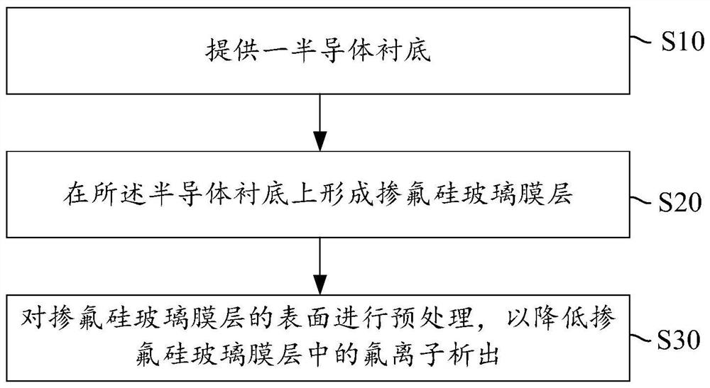
[0026] A semiconductor device and its forming method of the present invention will be further described in detail below. The invention will now be described in more detail with reference to the accompanying drawings, in which preferred embodiments of the invention are shown, it being understood that those skilled in the art may modify the invention described herein and still achieve the advantageous effects of the invention. Therefore, the following description should be understood as the broad knowledge of those skilled in the art, but not as a limitation of the present invention.

[0027] In the interest of clarity, not all features of an actual implementation are described. In the following description, well-known functions and constructions are not described in detail since they would obscure the invention with unnecessary detail. It should be appreciated that in the development of any actual embodiment, numerous implementation details must be worked out to achieve the de...


PUM


Abstract

The present invention provides a semiconductor device and its forming method. The forming method of the semiconductor device comprises the following steps: providing a semiconductor substrate; forming a fluorine-doped silicon glass film layer on the semiconductor substrate; Pretreatment to reduce the precipitation of fluoride ions in the fluorine-doped silicon glass film layer. The present invention pretreats the surface of the fluorine-doped silicate glass film layer, so that the dangling bonds on the surface of the fluorine-doped silicate glass film layer are saturated with oxygen atoms in hydrogen peroxide, thereby passivating the surface of the fluorine-doped silicate glass film layer, and then The speed of fluorine ion precipitation in the fluorine-doped silicon glass film layer is reduced, so that the waiting time between the deposition of FSG, chemical mechanical polishing and the formation of the subsequent covering layer of the fluorine-doped silicon glass film layer does not need to be controlled. The crystal defects that appear improve the reliability of the device, and at the same time, also reduce the process of rework or cleaning, reduce the process time, and improve the process efficiency.

Description

technical field [0001] The invention relates to the field of semiconductor manufacturing, in particular to a semiconductor device and a forming method. Background technique [0002] Fluorinated Silicate Glass (FSG: Fluorinated Silicate Glass) is widely used as a material in the back-end technology of integrated circuit manufacturing. It has low dielectric constant, good hole filling performance and stable mechanical constant. It has gradually replaced undoped silicon oxide ( USG) becomes the dielectric layer for interlayer isolation. However, due to the hydrophilicity of FSG, it is easy to absorb water vapor in the air to generate crystal defects, which affects the reliability of the device. [0003] The traditional solution is to control the waiting time between the deposition of FSG, chemical mechanical polishing, and the formation of the subsequent covering layer, thereby reducing the interval time in the preparation process steps. However, if the waiting time exceeds th...

Claims


Application Information

Patent Timeline
Patent Type & Authority Patents(China)
IPC IPC(8): H01L21/3105H01L21/768
CPCH01L21/3105H01L21/76822H01L21/76826
Inventor 胡海天田守卫李正阶朱朕
Owner SHANGHAI HUAHONG GRACE SEMICON MFG CORP
Why Eureka
Try Eureka