Method of producing gallium nitride-based III-V Group compound semiconductor device

a gallium nitride and compound semiconductor technology, applied in semiconductor/solid-state device manufacturing, semiconductor devices, electrical equipment, etc., can solve the problems of high p-type layer impedance, ineffective improvement of efficiency and impedance of ohmic contact, and difficulty in reducing the effect of p-type layer impedan

Inactive Publication Date: 2001-10-16
ARIMA OPTOELECTRONICS
View PDF2 Cites 4 Cited by
  • Summary
  • Abstract
  • Description
  • Claims
  • Application Information

AI Technical Summary

Problems solved by technology
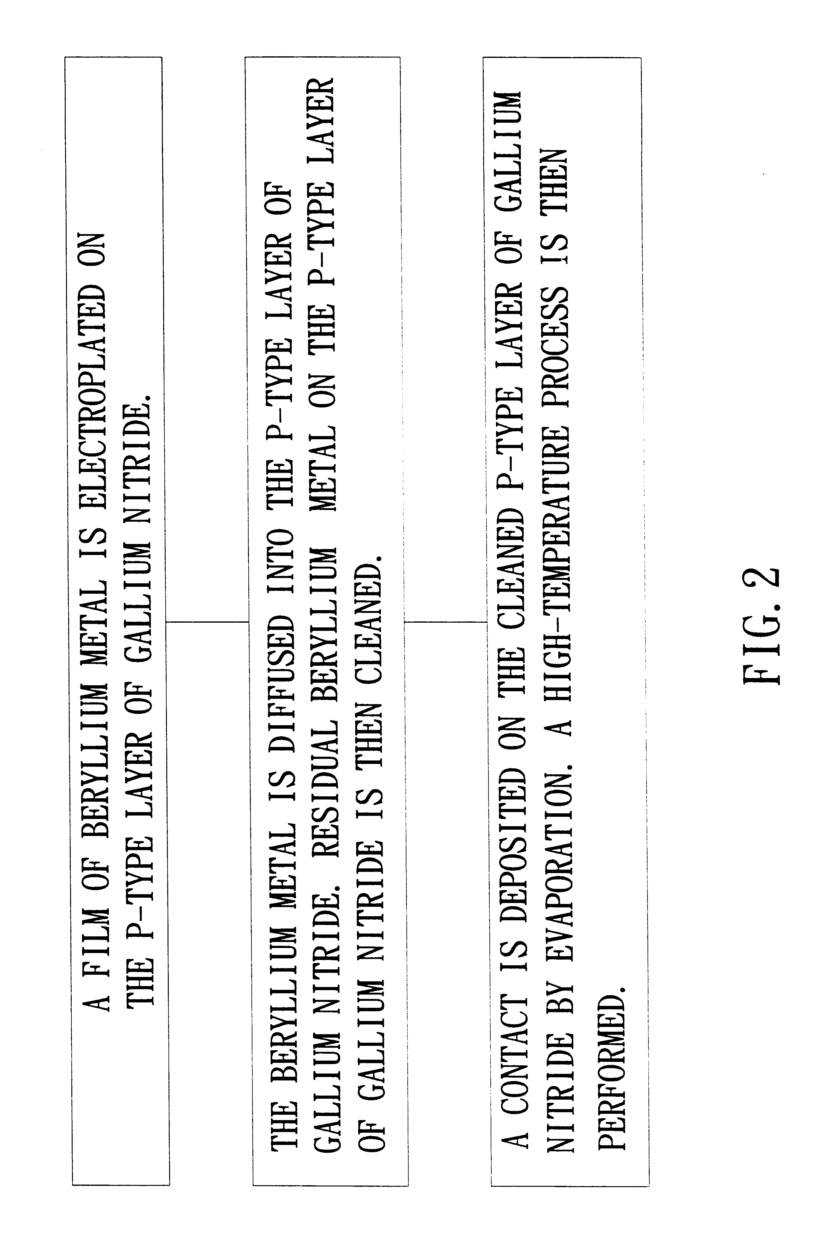
However, because the Al.sub.2 O.sub.3 substrate can not conduct electricity, in producing a device such as a light-emitting diode (LED), its p-contact and n-contact must be fabricated on the same surface and connected to the p-type layer and the n-type layer of the LED via an ohmic contact layer, respectively.
Moreover, the hole mobility of the p-type layer of gallium nitride-based III-V Group compound semiconductor device is low, resulting in a high impedance of the p-type layer.
Therefore, the diffusion of the hole current becomes an issue in the production of this device.
However, for metals such as nickel, chromium, aluminum, and gold on the p-type layer of gallium nitride, the efficiency and impedance of the ohmic contact can not be effectively improved.

Method used


Image

  • Method of producing gallium nitride-based III-V Group compound semiconductor device
  • Method of producing gallium nitride-based III-V Group compound semiconductor device
  • Method of producing gallium nitride-based III-V Group compound semiconductor device

Examples


Embodiment Construction

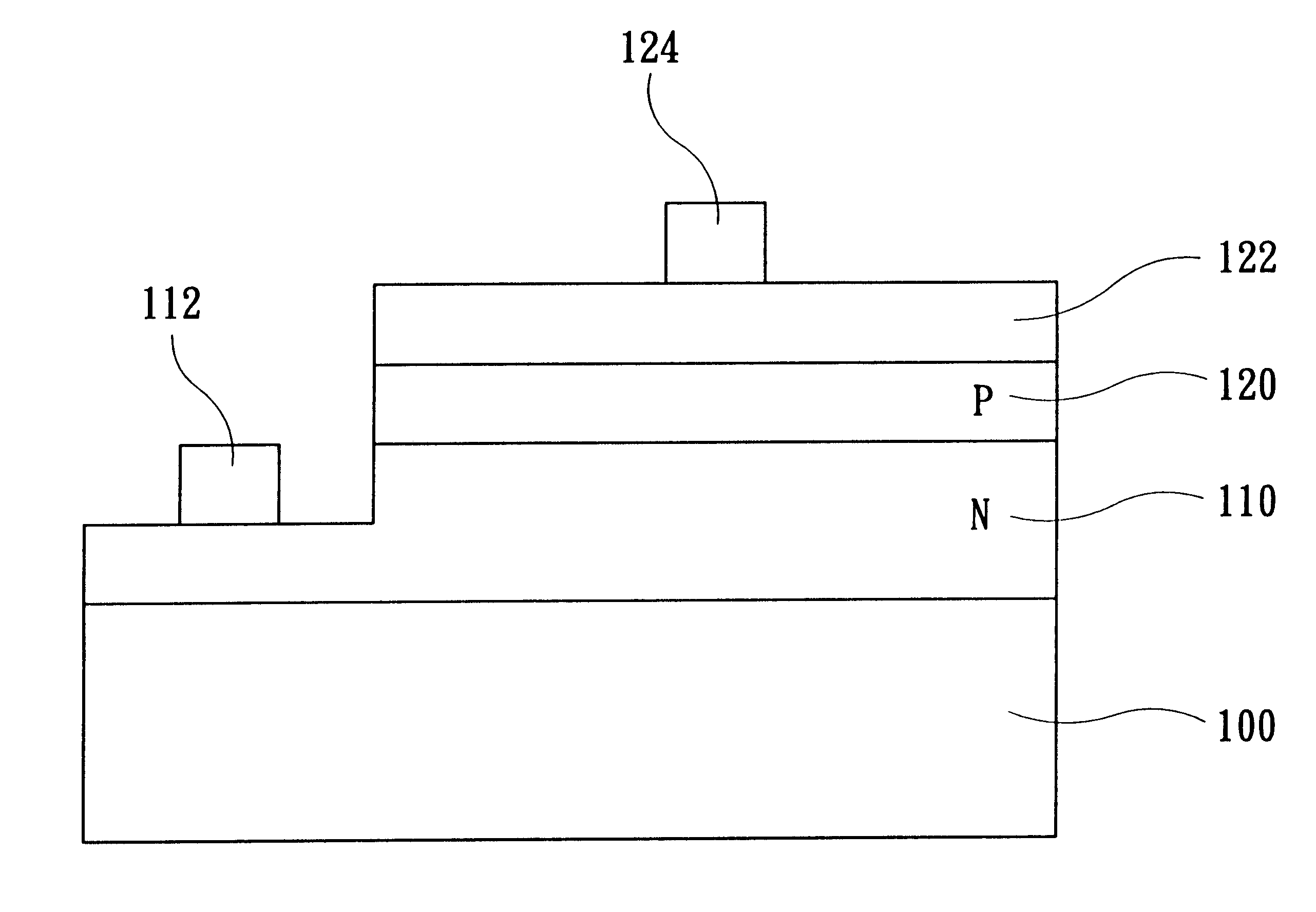
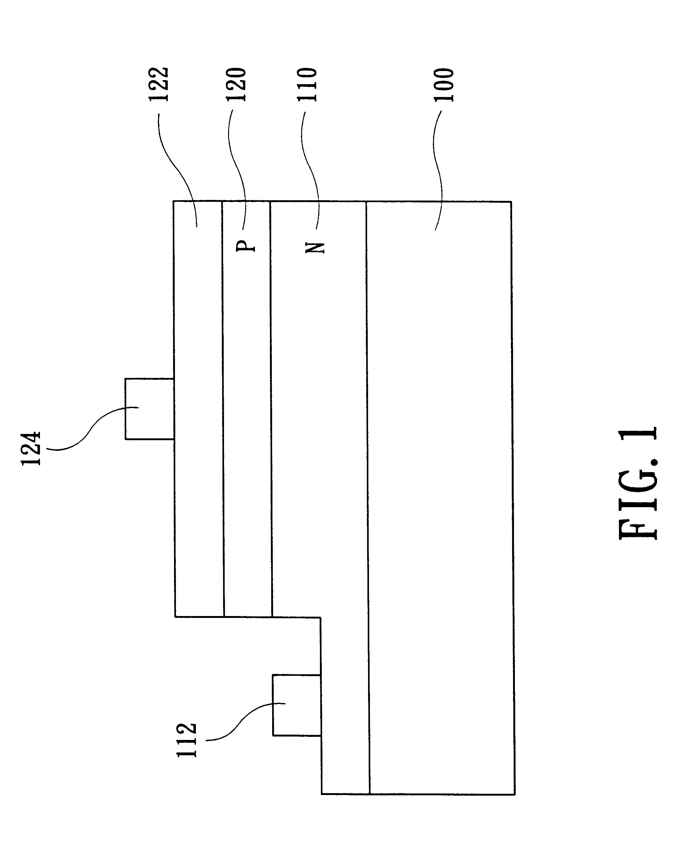
FIG. 1 is a cross-sectional view showing the structure of a device according to the present invention. The present invention aims to improve the method of fabricating the p-contact of a gallium nitride-based III-V Group compound semiconductor device (e.g., a gallium nitride-based LED). As shown in FIG. 1, a gallium nitride-based LED comprises mainly a substrate 100, an n-type layer of gallium nitride 110 on the substrate 100, and a p-type layer of gallium nitride 120 superposed on the n-type layer of gallium nitride 110. The substrate 100 can be an Al.sub.2 O.sub.3 single-crystal substrate so as to achieve better efficiency. Because this kind of substrate can not conduct electricity, the contacts of the LED must be fabricated on the front surface of the LED. As shown in FIG. 1, after the n-type layer of gallium nitride 110 and the p-type layer of gallium nitride 120 superposed thereon are formed, the n-type layer of gallium nitride 110 and the p-type layer of gallium nitride 120 sup...


PUM

PropertyMeasurementUnit
temperatureaaaaaaaaaa
thicknessaaaaaaaaaa
thicknessaaaaaaaaaa

Abstract

The present invention proposes a method of producing a gallium nitride-based III-V Group compound semiconductor device. First, beryllium ions are diffused into the p-type layer of gallium nitride to increase hole mobility. Contacts are then added in subsequent procedures, thereby forming contacts having low-impedance ohmic contact layers.

Description

The present invention relates to a method of producing a gallium nitride-based III-V Group compound semiconductor device.Compound semiconductor devices have been widely used in communication and for display. Due to recent requirement of blue light sources, gallium nitride-based III-V Group compound semiconductor devices have become the center of research and development. Gallium nitride-based III-V Group compound semiconductor devices generally comprise InGaN, GaAlN, and InAlGaN. The most efficient substrate used to grow gallium nitride-based III-V Group compound semiconductor devices is Al.sub.2 O.sub.3 single-crystal substrate. However, because the Al.sub.2 O.sub.3 substrate can not conduct electricity, in producing a device such as a light-emitting diode (LED), its p-contact and n-contact must be fabricated on the same surface and connected to the p-type layer and the n-type layer of the LED via an ohmic contact layer, respectively. The contact is generally made of metallic mater...

Claims


Application Information

Patent Timeline
Patent Type & Authority Patents(United States)
IPC IPC(8): H01L33/00
CPCH01L33/007Y10S438/93
Inventor SUNG, YING CHELIU, WENG MING
Owner ARIMA OPTOELECTRONICS
Why Eureka
Try Eureka