Dual nitrogen implantation techniques for oxynitride formation in semiconductor devices

a technology of oxynitride and nitride, which is applied in the manufacturing of semiconductor/solid-state devices, basic electric elements, electric devices, etc., can solve the problems of limiting the scaling of technology, and sti being more complicated and costly than conventional locos isolation, so as to prevent the threshold voltage of the nmos device

Inactive Publication Date: 2001-11-27
BELL SEMICON LLC
View PDF17 Cites 91 Cited by
  • Summary
  • Abstract
  • Description
  • Claims
  • Application Information

AI Technical Summary

Benefits of technology

To achieve the foregoing, the present invention provides a technique for fabrication of a nitrided gate oxide and STI oxide liner in a semiconductor device. One application of the present invention is to suppress both boron penetration into STI oxide and the RNCE in CMOS devices by introducing nitrogen to the STI edges of the p-well. This technique improves isolation performance and is also effective to harden the oxide. Nitridization of the STI liner may be conducted on its own or in combination with gate oxide nitridization, both with beneficial effect with regard to the RNCE. The nitridization may also be focussed on the channel region of the gate oxide in particular in order to mitigate RSCE.
Where the CMOS is formed in accordance with the process described with reference to FIGS. 3A-3F, the STI sidewalls and the substrate surface over the p-well have been implanted with nitrogen to form continuous oxynitride 512 and silicon nitride 514 layers. This provides nitridization at the channel surface that prevents the diffusion of boron to the channel surface towards the conventional gate oxide, and thereby prevents the threshold voltage for the NMOS device of the CMOS 500 from getting any higher. The nitridization of the gate oxide retards the diffusion of boron from the polysilicon gate electrode towards the gate oxide into the channel region of the PMOS device, and thereby prevents the threshold voltage of the PMOS device from getting lowered ("boron penetration").

Problems solved by technology

However, STI is more complicated and costly compared to the conventional LOCOS isolations.
Therefore, much like "bird's beak" in LOCOS, these problems limit the scaling of the technology.
A further problem encountered with shallow trench isolations is the so-called reverse narrow channel effect (RNCE), or reverse narrow width effect (RNWE).
This RNCE results in difficulties in, for example, design of embedded memory devices.
RNCE frustrates transistor designers' general preference to keep voltage threshold profiles relatively flat over the width of a transistor so that a transistor will work with approximately the same threshold voltage regardless of its width and length.
This makes the transistor harder to invert requiring a higher threshold voltage to get the same inversion.

Method used


Image

  • Dual nitrogen implantation techniques for oxynitride formation in semiconductor devices
  • Dual nitrogen implantation techniques for oxynitride formation in semiconductor devices
  • Dual nitrogen implantation techniques for oxynitride formation in semiconductor devices

Examples


Embodiment Construction

The following example provides details concerning techniques and structures which demonstrate an implementation in accordance with the present invention. It should be understood the following is representative only, and that the invention is not limited by the detail set forth in this example.

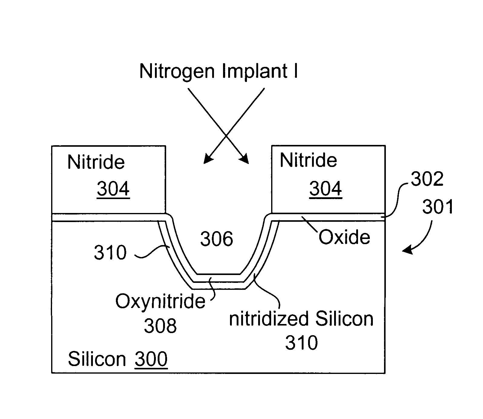
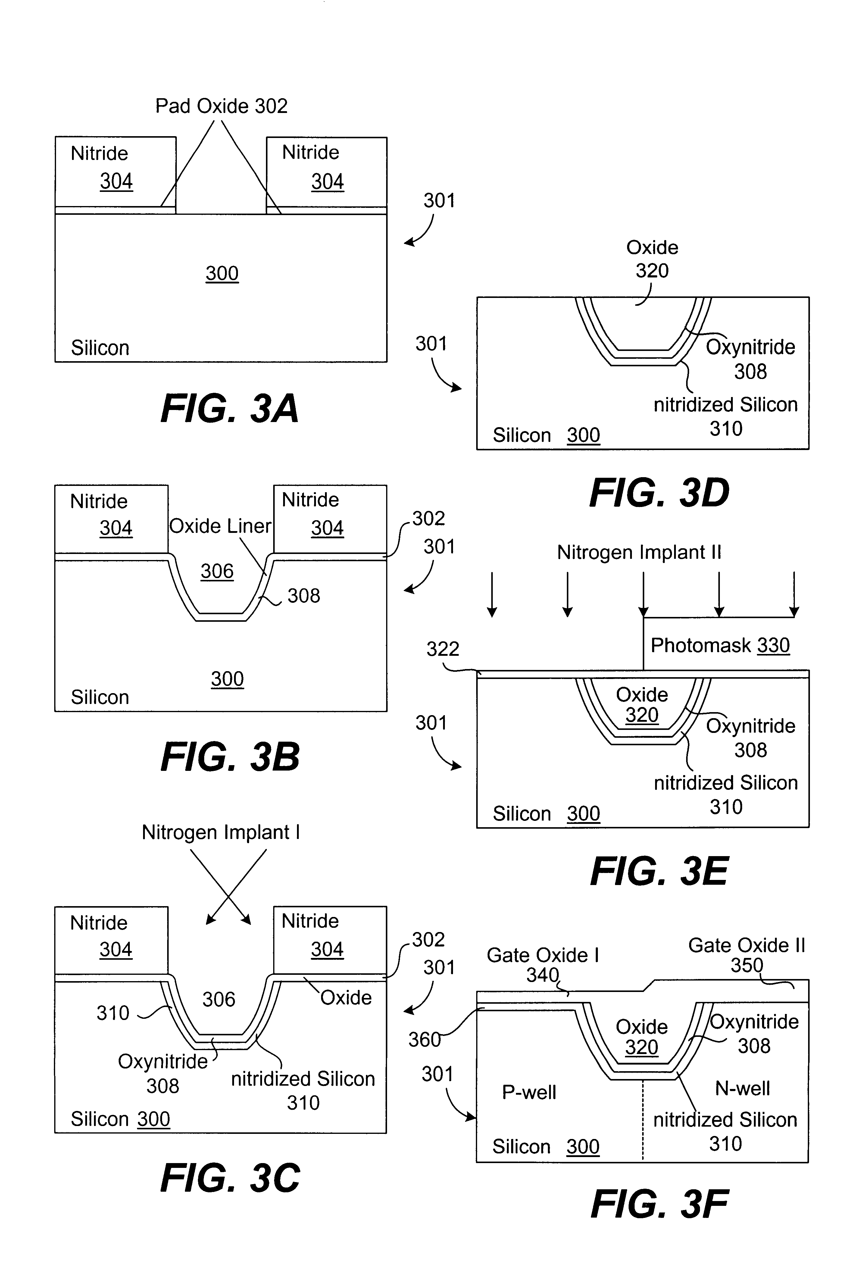
Shallow trenches (0.253 .mu.m and 0.4 .mu.m deep) were etched into a silicon substrate using a nitride / oxide hard mask, and followed by a short high temperature liner oxidation. The trench was filled with a HDP-CVD, and followed by a CMP planarization down to the nitride layer, which was subsequently removed by hot phosphoric acid. Retrograde wells were done afterwards. A nitrogen-rich layer was introduced to the Si / SiO.sub.2 interface at trench edge by implanting nitrogen at 25 keV with a dose of 4e14 and 5e14 cm.sup.-2 through a screen oxide. Gate oxide growth followed. Then a polysilicon layer was deposited and doped. Standard back-end process was carried out to metal one.

The experimental da...


PUM


Abstract

Provided is a technique for fabrication of a nitrided gate oxide and shallow trench isolation (STI) oxide liner in a semiconductor depletion into STI oxide and the RNCE in CMOS devices by introducing nitrogen to the STI edges of the p-well. This technique improves isolation performance and is also effective to harden the oxide to reduce boron penetration. Nitridization of the STI liner may be conducted on its own or in combination with gate oxide nitridization, both with beneficial effect with regard to the RNCE. The nitridization may also be focussed on the channel region of the gate oxide in particular in order to mitigate RSCE.

Description

The present invention relates to nitrogen implantation schemes for creating oxynitride gates of variable thicknesses and / or an oxynitride liner for shallow trench isolation in semiconductor devices.Integrated Circuit (IC) technology relies on the successful performance of each of its contributing components. Although the technology drivers are typically high performance active devices, the overall success of an IC technology hinges equally critically on good isolation structures (areas that prevent the active devices from interfering with each other). A variety of techniques have been developed to isolate devices in integrated circuits. Among the different isolation structures, shallow trench isolation (STI) has long been viewed as the indispensable device isolation for deep sub-micron technology, because it is free from bird's beak encroachment, field oxide thinning and leakage due to punchthrough. However, STI is more complicated and costly compared to the conventional LOCOS isola...

Claims


Application Information

Patent Timeline
Patent Type & Authority Patents(United States)
IPC IPC(8): H01L21/762H01L21/70H01L21/02H01L21/265H01L21/8234
CPCH01L21/26586H01L21/76232H01L21/823462H01L21/823481H01L21/26506
Inventor HUANG, SHIH-FENPUCHNER, HELMUT
Owner BELL SEMICON LLC
Why Eureka
Try Eureka