Transportation method for substrate wafers and transportation apparatus

a technology of transportation apparatus and substrate, which is applied in the direction of instruments, furniture, programme control, etc., can solve the problems of inability to precisely form an amolphous silicon (a-si) film with uniform thickness on top, difficulty in manufacturing a high quality product, and manufacturing steps

Inactive Publication Date: 2002-01-29
NIPPON SANSO CORP
View PDF9 Cites 190 Cited by
  • Summary
  • Abstract
  • Description
  • Claims
  • Application Information

AI Technical Summary

Problems solved by technology

An extremely high degree of precision is required in the manufacture of each of these products, and if only a slight amount of impurity adheres to or is absorbed by the surface of the processed substrates, that is, the substrate wafer, it is difficult to manufacture a high quality product.
For example, if water, an impurity such as moisture, is absorbed by the surface of a semiconductor substrate during a manufacturing step, it will cause a hindrance to the manufacturing step.
In addition, in the manufacturing steps of the thin film transistor (TFT) used in liquid crystal panels, if there is water on the surface of the insulating film made, for example, of SiN.sub.x, it is impossible to precisely form an amolphous silicon (a-Si) film with uniform thickness on top of it.
Similarly, if there is water on the surface of a capacitor, an SiO.sub.x film will form in its interface making it impossible to charge the capacitor electrode, and it will not function as a memory device.
In addition, in order to prevent spiking due to tungsten silicide in the wiring process, a TiN film is formed before depositing a tungsten (W) film, but if there is water on the substrate, problems such as the deterioration of the adhesiveness of the TiN film occur.
Furthermore, when there are impurities other then water, for example, organic impurities such as methane, during heat processing, the silicon reacts with the carbon on the surface of the substrate (silicon), forming an SiC film, and problems are caused in the operating characteristics of the device.
When trying to prevent the abs

Method used


Image

  • Transportation method for substrate wafers and transportation apparatus
  • Transportation method for substrate wafers and transportation apparatus
  • Transportation method for substrate wafers and transportation apparatus

Examples


embodiment

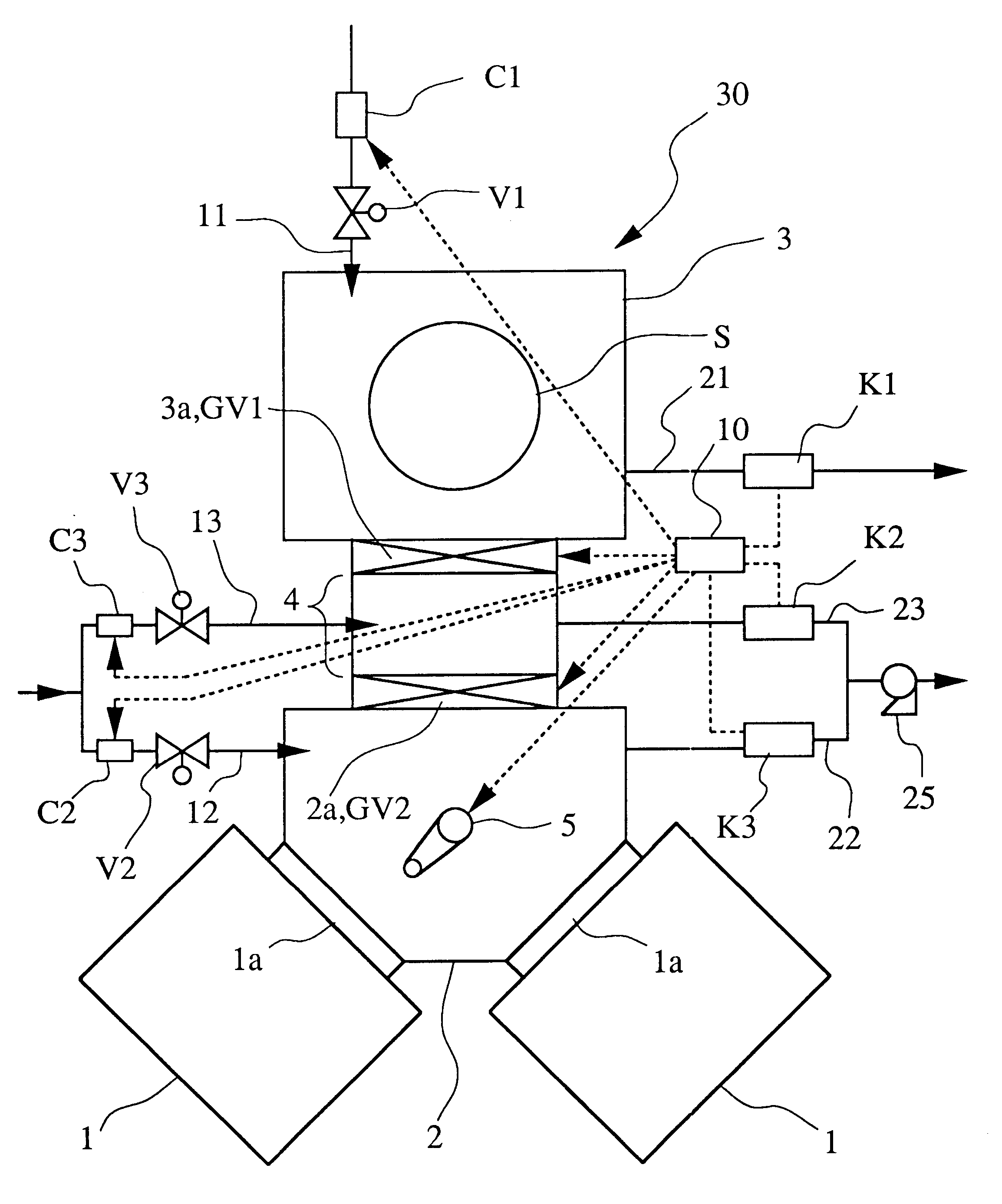
Transportation of the substrate wafer S was carried out using the transportation apparatus of the present Invention, and the presence of native oxide film and the amount of organic contaminants was measured.

These measurements were carried out under the following conditions:

(2) Resistance value of the substrate wafer:

2.about.4 .OMEGA..multidot.cm, n-type (100) silicon substrate surface area: 1.41.times.10.sup.3 cm.sup.2 / sheet.times. 25 sheets= 3.53.times.10.sup.4 cm.sup.2.

The following results of the ratio of impurities were obtained from the results of measurement by semiconductor laser detectors K1, K2, and K3:

(3) Ratio of impurities

Under these conditions, carrying out experimental transportation of a substrate wafer S from storage box 3 to transportation box 2, neither a native oxide film nor absorption of organic contaminants on the surface of the substrate wafer S returned to the storage box 3 was detected by X-ray photoelectron spectroscopy or FT-IR (Fourier transform infrared...


PUM


Abstract

The present invention uses a transportation robot furnished with a storage chamber 3 that can store substrate wafers S under an inert gas atmosphere, and when transporting substrate wafers S between transportation chambers 2 installed on processing apparatus 1 and holding an inert gas atmosphere, connection chamber 4 is disposed between storage chamber 3 and transportation chamber 2 when placing and removing substrate wafers S between storage chamber 3 of transportation robot 30 and the transportation chamber 2 of processing apparatus 1, and after introducing inert gas into the connection chamber 4 at low pressure, opening the gate valves GV1 and GV2 between storage chamber 3 and transportation chamber 2.

Description

The present invention relates to a transportation method and transportation apparatus using a transport robot for transporting between processing steps substrate wafers used, for example, in semiconductor integrated circuits, liquid crystal displays panels, solar battery panels.This application is based on patent application No. Hei 8-315193 filed in Japan, the content of which is incorporated herein by reference.DESCRIPTION OF RELATED ARTSemiconductor elements such as semiconductor integrated circuits and semiconductor lasers, active matrix type liquid crystal display panels, solar battery panels, etc., are manufactured by a process of laminating in sequence various predetermined thin films on a silicon substrate, gallium arsenide substrate, glass substrate, etc. whose surfaces are highly cleaned. An extremely high degree of precision is required in the manufacture of each of these products, and if only a slight amount of impurity adheres to or is absorbed by the surface of the pro...

Claims


Application Information

Patent Timeline
IPC IPC(8): H01L21/67H01L21/677B65G49/00B65G49/07
CPCH01L21/67126H01L21/67736H01L21/67724H01L21/68
Inventor TODA, MASAYUKIOHMI, TADAHIROISHIHARA, YOSHIO
Owner NIPPON SANSO CORP
Why Eureka
Try Eureka