Introducing catalytic and gettering elements with a single mask when manufacturing a thin film semiconductor device

a semiconductor device and catalytic element technology, applied in the direction of semiconductor devices, electrical devices, transistors, etc., can solve the problems of reproducibility and stability, the change of the characteristics of the obtained semiconductor device with the lapse of time, and the dispersion of off values

Inactive Publication Date: 2002-02-19
SEMICON ENERGY LAB CO LTD
View PDF9 Cites 122 Cited by
  • Summary
  • Abstract
  • Description
  • Claims
  • Application Information

AI Technical Summary

Problems solved by technology

Since such a driver circuit and a logic circuit are required to perform high speed operation, it is improper to use an amorphous silicon film as an active layer.
Although it becomes possible to obtain a silicon film having excellent crystallinity by the above crystallizing technique at a relatively low temperature, since the catalytic element is included in the film, the control of the amount of the addition is subtle, and a problem has occurred in the reproducibility and stability (stability in electrical characteristics of a device obtained).
Besides, there has also occurred a problem that change of characteristics of the obtained semiconductor device with the lapse of time and the dispersion of OFF values (off current) as characteristic values of the TFT are large by the influence of the catalytic element remaining in the film.

Method used


Image

  • Introducing catalytic and gettering elements with a single mask when manufacturing a thin film semiconductor device
  • Introducing catalytic and gettering elements with a single mask when manufacturing a thin film semiconductor device
  • Introducing catalytic and gettering elements with a single mask when manufacturing a thin film semiconductor device

Examples


embodiment 1

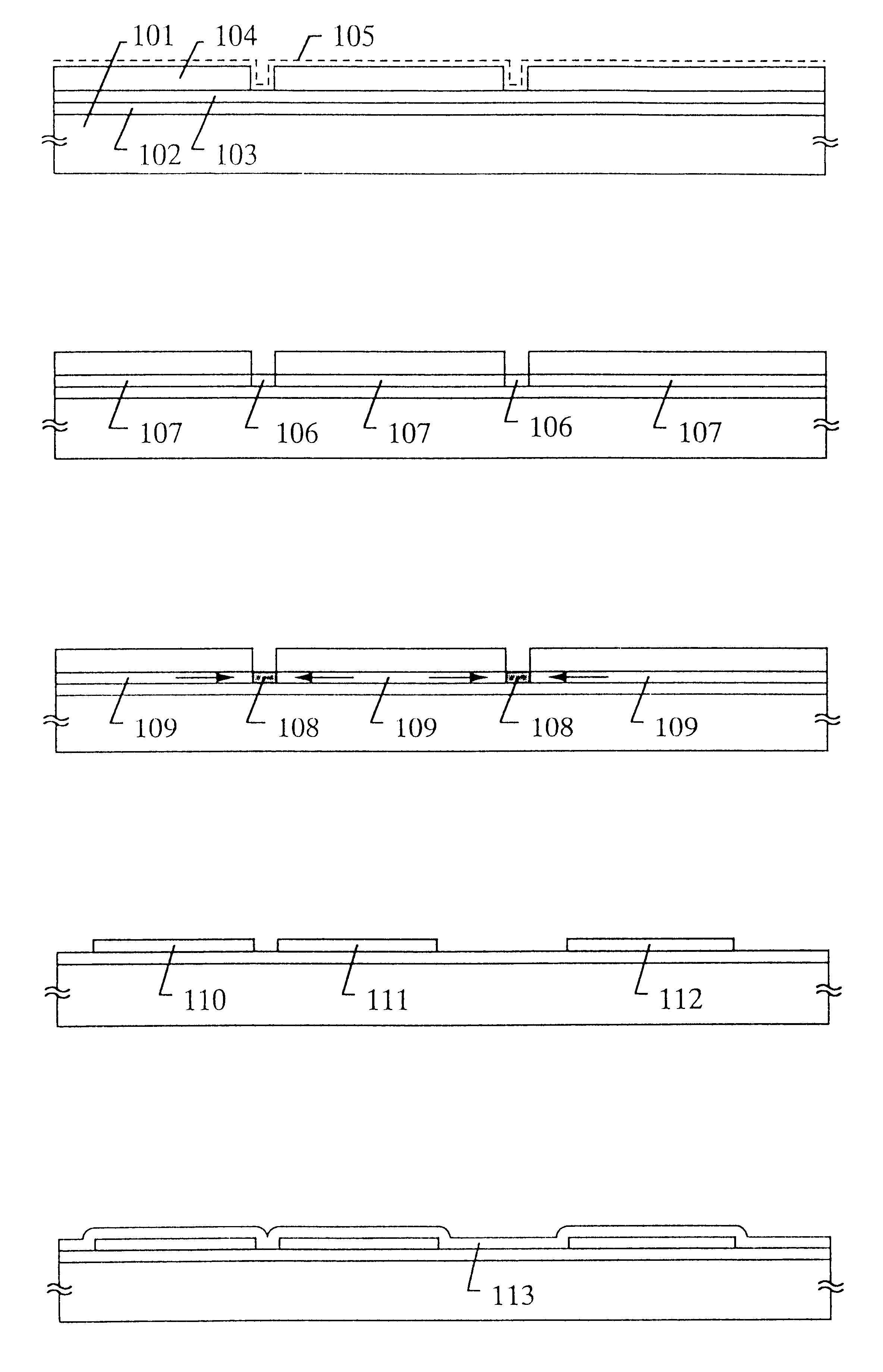
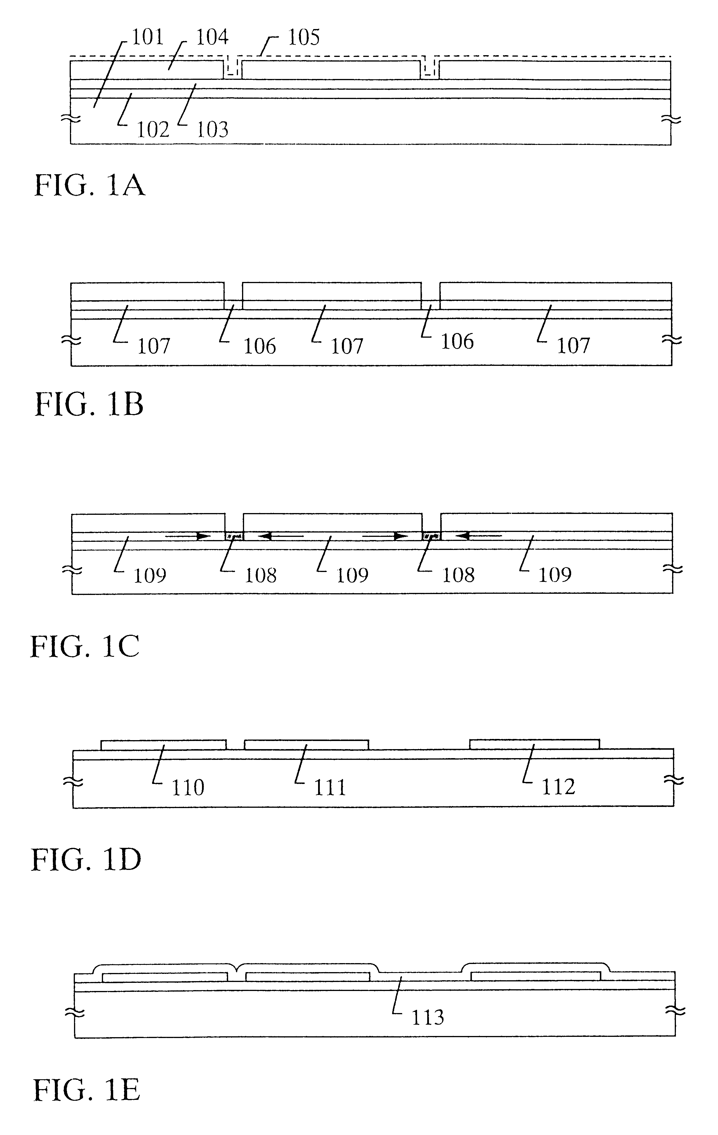
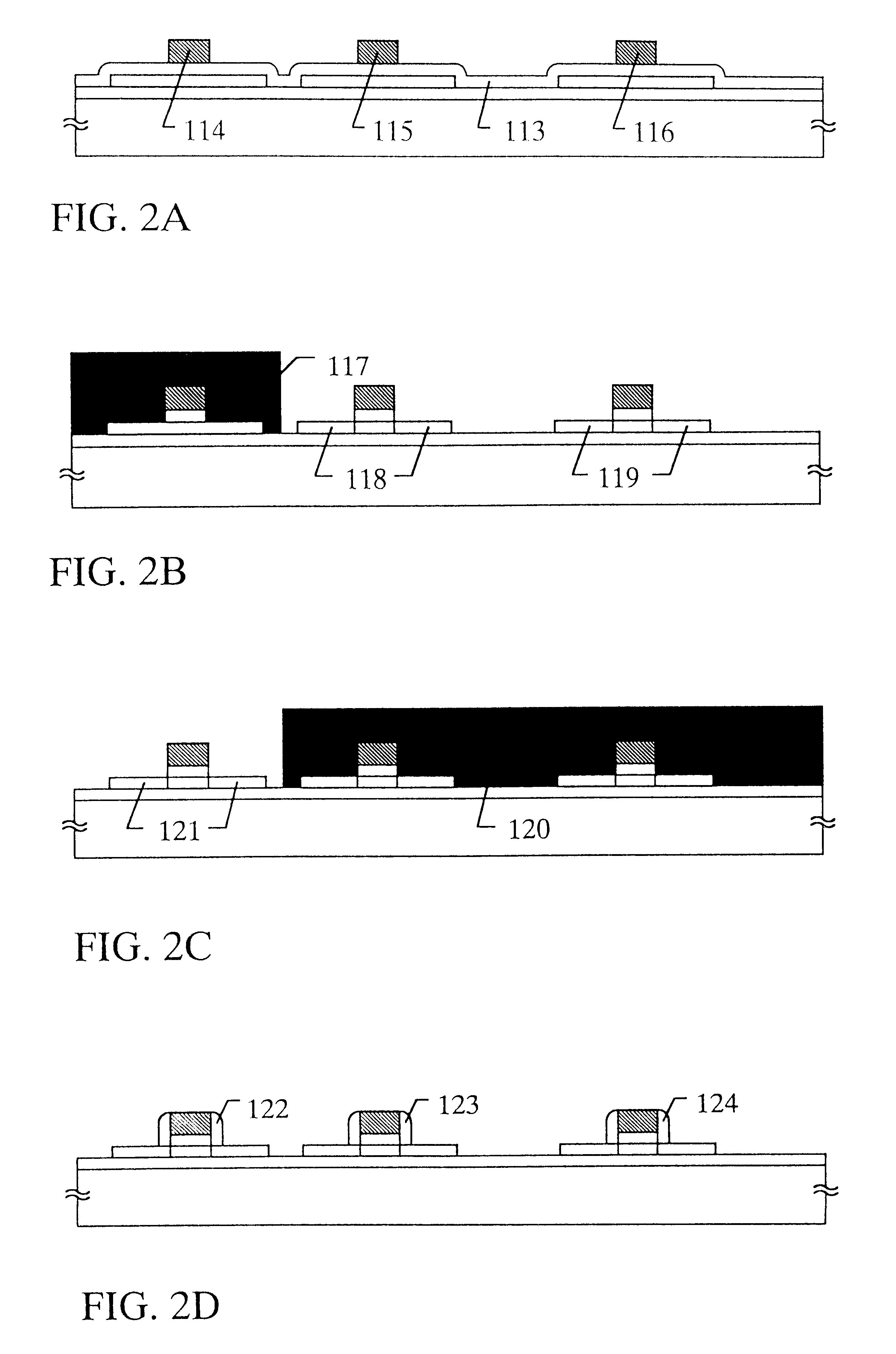
Incidentally, it is very effective in decreasing defects within a crystal grain to carry out the annealing step (step shown in FIG. 1E) at a temperature above the crystallizing temperature when the semiconductor thin film of the present invention is formed as in the This will be described below.

FIG. 11A is a TEM photograph showing a crystalline silicon film manufactured in accordance with the embodiment 1, magnified one million times. Defects due to lamination defects or dislocations are hardly seen in the crystal grain, and it is understood that the crystallinity is very high. This tendency can be seen in the entire of the film surface, and although it is difficult to reduce the number of defects to zero in the present circumstances, it is possible to reduce the number to substantially zero.

That is, in the crystalline silicon film shown in FIG. 11A, the defects in the crystal grain are reduced to the degree that the defects can be almost neglected, and the crystal grain boundary c...

embodiment 2

In this embodiment, an example in which a crystallizing step of an amorphous silicon film is carried out by a means different from the embodiment 1 will be described with reference to FIGS. 8A to 8E. Concretely, the example in which there is employed the means as disclosed in embodiment 1 of Japanese Patent Laid-open No. 7-130652 will be described.

First, a silicon oxide film 802 with a thickness of 200 nm is formed on a quartz substrate 801. Then an amorphous silicon film 803 with a thickness of 75 nm is formed thereon by a low pressure CVD method. A nickel acetate solution containing nickel of 10 ppm in weight is applied by a spin coating method to form a nickel containing layer 804 (FIG. 8A).

Next, after dehydrogenating is carried out at 500.degree. C. for one hour, a heat treatment is carried out at 550.degree. C. for 4 hours to form a crystalline silicon film 805. At this time, excimer laser annealing may be carried out after crystallization to crystalize remaining amorphous comp...

embodiment 3

In this embodiment, an example in which crystallized glass is used for the substrate in the embodiment 1, and an insulating silicon film formed by a low pressure CVD method is used as a protective film (serving also as an under film) for protecting the glass substrate, will be described with reference to FIG. 4.

In the case of this embodiment, crystallized glass containing ingredients of SiO.sub.2 : 52.5, Al.sub.2 O.sub.3 : 26.5, MgO: 11.9, and TiO.sub.2 : 11.4 is prepared as a substrate 401. This is nonalkaline cordierite crystallized glass using TiO.sub.2 as a nucleus forming agent.

Next, an insulating silicon film 402 capable of functioning as a protective film is formed on the front surface, rear surface, and side surface of the crystallized glass. In this embodiment, a silicon nitride oxide film is formed by a low pressure CVD method using silane (SiH.sub.4) and nitrous oxide (N.sub.2 O) as a film forming gas.

In this case, the film forming temperature is made 800 to 850.degree. C...


PUM


Abstract

In a method of manufacturing a semiconductor device, after a lateral growth region 107 is formed by using a catalytic element 105 for facilitating crystallization of silicon, the catalytic element is gettered into a phosphorus added region 108 by a heat treatment. Thereafter, a gate insulating film 113 is formed to cover active layers 110 to 112 formed, and in this state, a thermal oxidation step is carried out. By this, the characteristics of an interface between the active layers and the gate insulating film can be improved while abnormal growth of a metal oxide is prevented.

Description

1. Field of the InventionThe present invention relates to a method of manufacturing a semiconductor device using a semiconductor thin film, and particularly to a method of manufacturing a semiconductor device constituted by a thin film transistor (TFT) using a crystalline silicon film.In the present specification, "semiconductor" device means any device functioning by using a semiconductor, and not only a simple component such as a TFT but also an electro-optical device, a semiconductor circuit, and electronic equipment provided with those.2. Description of the Related ArtIn recent years, a TFT used for an electro-optical device such as an active matrix type liquid crystal display device has been actively developed.The active matrix type liquid crystal display device is a monolithic display device in which a pixel matrix circuit and a driver circuit are provided on the same substrate. Moreover, a system-on-panel having built-in logic circuits, such as a y correction circuit, a memor...

Claims


Application Information

Patent Timeline
Patent Type & Authority Patents(United States)
IPC IPC(8): H01L21/02H01L29/66H01L21/20H01L21/322H01L29/786H01L21/336
CPCH01L21/2022H01L29/78675H01L21/3226H01L21/02686H01L21/02422H01L21/02488H01L21/02532H01L21/0242H01L21/02672H01L21/02381H01L21/42
Inventor YAMAZAKI, SHUNPEIOHTANI, HISASHI
Owner SEMICON ENERGY LAB CO LTD
Why Eureka
Try Eureka