Semiconductor device including ferroelectric capacitor

a technology of ferroelectric capacitors and semiconductors, which is applied in the direction of semiconductor devices, capacitors, electrical equipment, etc., can solve the problems of abnormal growth of crystals on the surface of films, abnormal growth of films having a thickness of 100 nm or more, and abnormal growth of films. to achieve the effect of suppressing abnormal growth and generating voids

Inactive Publication Date: 2008-02-14
FUJITSU SEMICON MEMORY SOLUTION LTD
View PDF6 Cites 16 Cited by
  • Summary
  • Abstract
  • Description
  • Claims
  • Application Information

AI Technical Summary

Benefits of technology

[0039]It is possible to suppress abnormal growth and generation...

Problems solved by technology

It has been found that a new problem occurs if the upper electrode of a ferroelectric capacitor is made of a first conductive oxide film having a suppressed oxidation degree and a second conductive oxide film having an increased oxidation degree.
However, as the second conductive oxide film having a high oxidation degre...

Method used


Image

  • Semiconductor device including ferroelectric capacitor
  • Semiconductor device including ferroelectric capacitor
  • Semiconductor device including ferroelectric capacitor

Examples


first embodiment

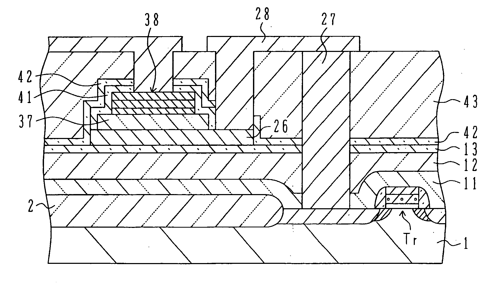
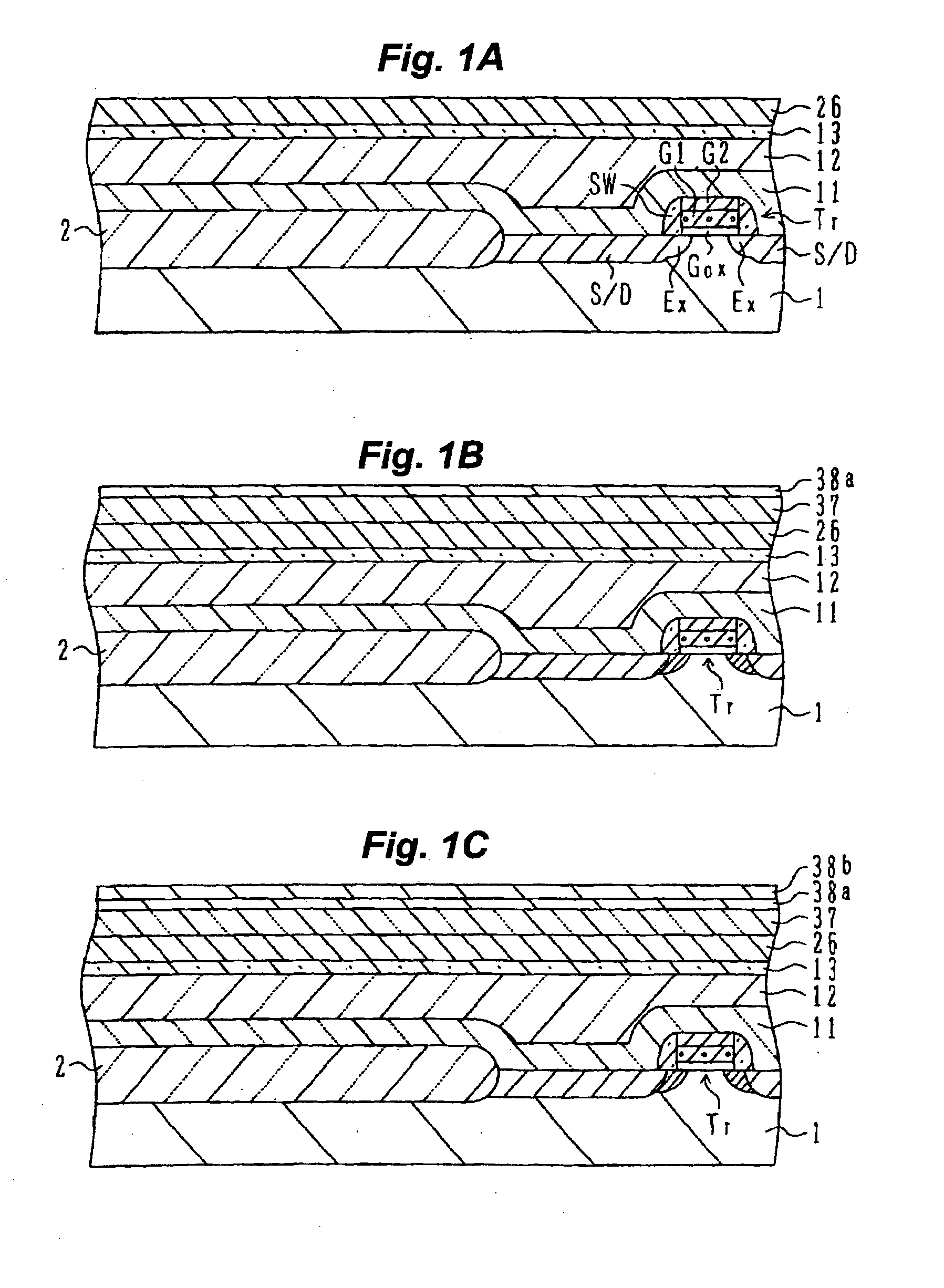
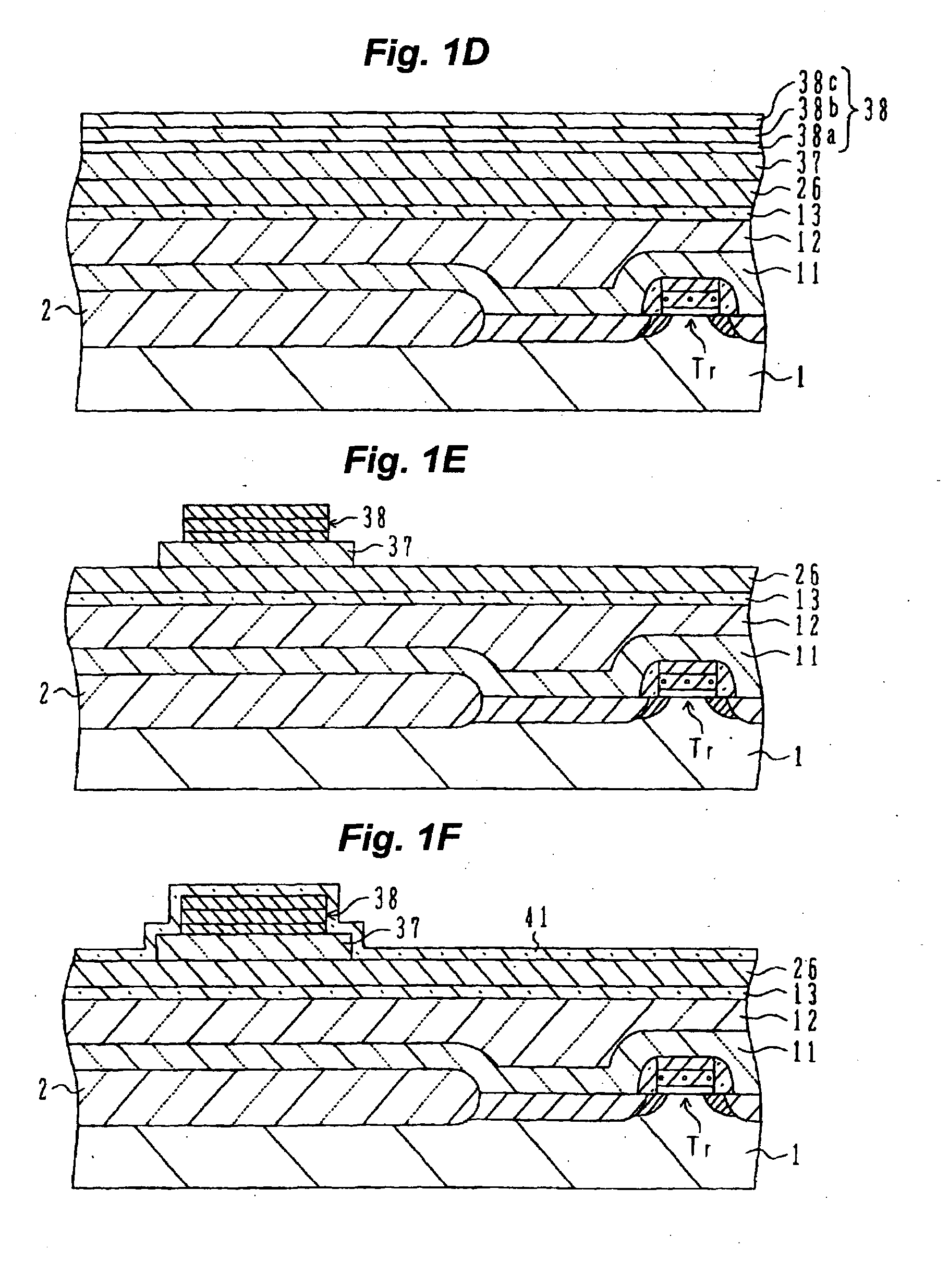
[0057]With reference to FIGS. 1A to 1L, description will be made on manufacture processes for a planar type FeRAM and a structure of the manufactured FeRAM, according to the present invention.

[0058]As shown in FIG. 1A, for example, on the surface of a p-type Si substrate 1, an isolation region 2 is formed, for example, by local oxidation of silicon (LOCOS) to define active regions. The surfaces of the active regions are thermally oxidized to form a silicon oxide film having a thickness of, e.g., about 10 nm to be used as a gate oxide film Gox. On the gate oxide film Gox, a polycide gate electrode G is formed which is a lamination of a first gate electrode G1 of polysilicon and a second gate electrode G2 of silicide. By using a resist pattern, the lamination is patterned to form the gate electrode G, and thereafter, n-type impurity ions, e.g., As, are implanted shallowly to form low concentration extension regions Ex.

[0059]After the extension regions are formed, an insulating film of...

second embodiment

[0113]With reference to FIGS. 3A to 3T, description will be made on a stack type FeRAM manufacture method according to the present invention.

[0114]As shown in FIG. 3A, an isolation trench is formed in a surface layer of a substrate 1 of n- or p-type silicon. After the trench surface is oxidized, a silicon oxide film is buried, for example, by high density plasma (HDP) CVD, and unnecessary regions are removed by CMP to form an isolation region 2 by shallow trench isolation (STI) and define active regions. The isolation region may be formed by LOCOS instead of STI. A p-type well 3 is formed by implanting p-type impurity ions into a surface layer of the active region.

[0115]A common source region of two MOS transistors is connected to a bit line, and a capacitor is connected to each drain to form two memory cells. This interconnect arrangement is widely used in DRAM. The embodiment also adopts this interconnect arrangement. Two MOS transistors 5 are formed in the active region. Brief de...


PUM


Abstract

A semiconductor device includes a ferroelectric capacitor formed above the lower interlevel insulating film covering a MOS transistor formed on a semiconductor substrate, including lamination of a lower electrode, an oxide ferroelectric film, a first upper electrode made of conductive oxide having a stoichiometric composition AOx1 and an actual composition AOx2, a second upper electrode made of conductive oxide having a stoichiometric composition BOy1 and an actual composition BOy2, where y2/y1>x2/x1, and a third upper electrode having a composition containing metal of the platinum group; and a multilayer wiring structure formed above the lower ferroelectric capacitor, and including interlevel insulating films and wirings. Abnormal growth and oxygen vacancies can be prevented which may occur when the upper electrode of the ferroelectric capacitor is made of a conductive oxide film having a low oxidation degree and a conductive oxide film having a high oxidation degree.

Description

CROSS REFERENCE TO RELATED APPLICATION[0001]This application is based on and claims priority of Japanese Patent Application No. 2006-218924 filed on Aug. 10, 2006, the entire contents of which are incorporated herein by reference.BACKGROUND OF THE INVENTION[0002]A) Field of the Invention[0003]The present invention relates to a semiconductor device and its manufacture method, and more particularly to a semiconductor device having ferroelectric capacitors and its manufacture method.[0004]B) Description of the Related Art[0005]With the recent development of digital technologies, there arise high demands for processing or storing a large amount of data at high speed. Therefore, semiconductor devices used in electronic apparatus are required to have high integration density and high performance. For example, in order to realize high integration density of dynamic random access memories (DRAMs), techniques are widely researched and developed by which a ferroelectric material film or a hig...

Claims


Application Information

Patent Timeline
IPC IPC(8): H01L29/94
CPCH01L21/32051H01L21/76826H01L21/76841H01L28/65H01L27/11502H01L27/11507H01L28/55H01L21/76883H10B53/30H10B53/00
Inventor WANG, WENSHENG
Owner FUJITSU SEMICON MEMORY SOLUTION LTD
Why Eureka
Try Eureka