

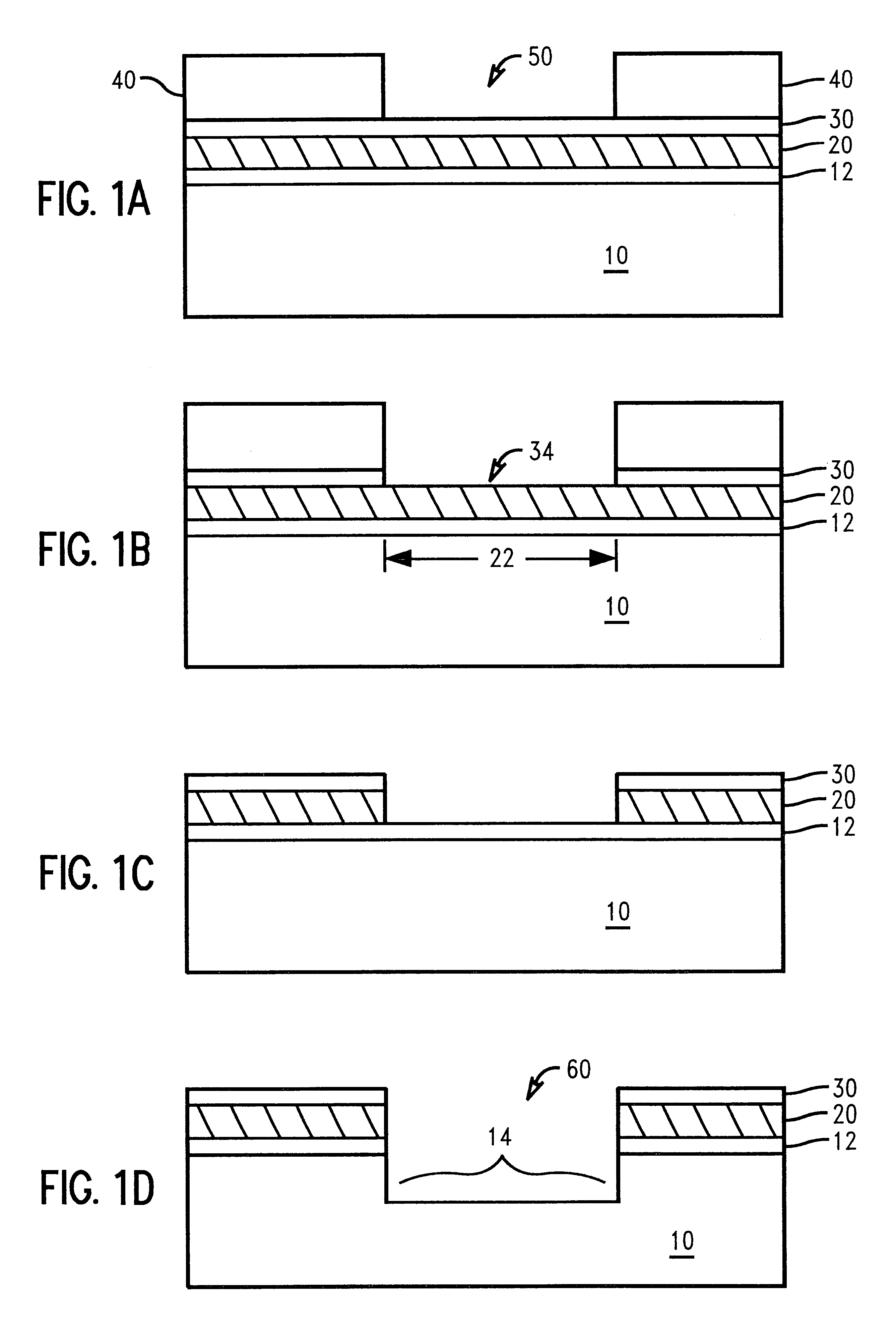
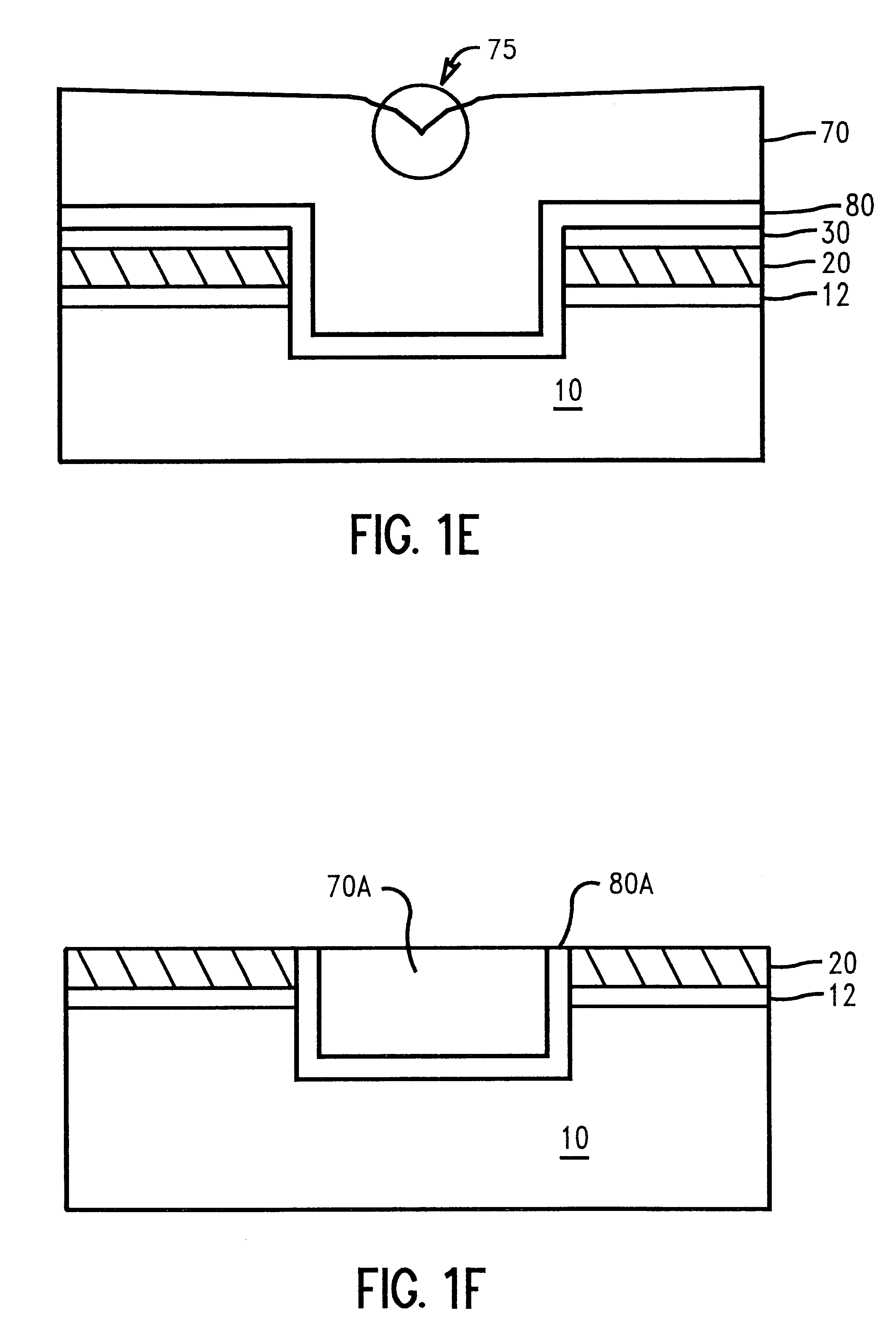
Diamond as a polish-stop layer for chemical-mechanical planarization in a damascene process flow
a technology of damascene and polishing layer, which is applied in the direction of semiconductor/solid-state device manufacturing, basic electric elements, electric apparatus, etc., can solve the problems of reducing the topography of the surface of the semiconductor, no known art reports the use of diamond or a diamond-like carbon material and the use of diamond or a diamond-like carbon material as disclosed in jaso would not be effective as a polishing layer. , to achieve the
- Summary
- Abstract
- Description
- Claims
- Application Information
AI Technical Summary
Benefits of technology
Problems solved by technology
Method used
Image

Examples
second embodiment
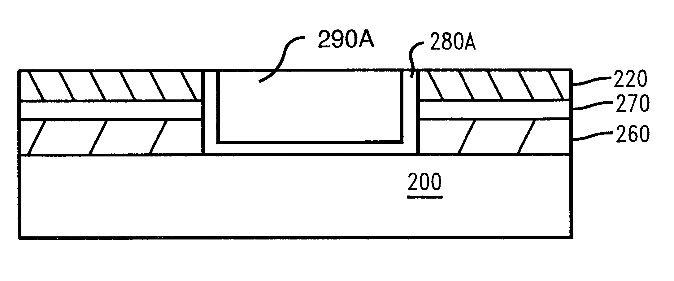
The second embodiment differs from the first in that an epitaxial growth process is performed in order to grow conductive layer 170 from the material comprising substrate 110, rather than applying a conductive material to form such conductive layer. In a preferred embodiment, an epitaxial growth process is carried out to grow semiconductor material from the substrate upward and over the diamond mask layer as shown in FIG. 2D. Such epitaxial growth may be performed by techniques known and used in the art. Such an epitaxial growth process forms excess substrate material at the surface of the semiconductor, as well as topography. A CMP process may be used to remove such excess and topography.
In the second embodiment, a chemical-mechanical polish process is carried out to remove the excessive semiconductor material using a basic SiO.sub.2 slurry. The pH of the slurry can be controlled with ammonium hydroxide, potassium hydroxide, and the like, and combinations thereof. Over-polish is ne...
PUM
 Abstract
Description
Claims
Application Information