In situ formation of protective layer on silsesquioxane dielectric for dual damascene process
- Summary
- Abstract
- Description
- Claims
- Application Information
AI Technical Summary
Benefits of technology
Problems solved by technology
Method used
Image

Examples
Embodiment Construction
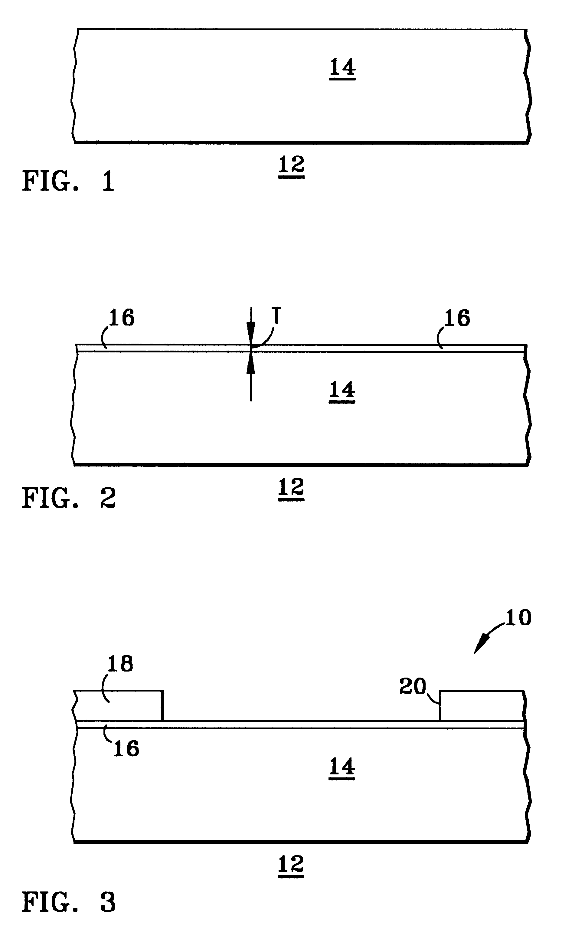
Referring now to the figures and more particularly to FIG. 1, there is shown an SSQ dielectric layer 14 disposed on an integrated circuit chip 12 rior to dual Damascene processing.
FIG. 2 shows a thin oxide dielectric layer 16 formed according to the present invention. Preferably, the layer 16 is formed in situ by exposing the SSQ dielectric layer 14 to an oxygen-containing plasma in a suitable processing apparatus (not shown). After formation, the layer 16 preferably is (SiO.sub.2). Any suitable commercially available plasma chamber apparatus can be used, such as a Precision 5000, manufactured by Applied Materials. Preferably, the processing parameters for forming the layer 16 are in the following ranges: 8 to 14 torr pressure, 300 to 1000 W power, 100 to 1000 sccm O2, 350 to 400 C temperature, 1 to 30 seconds process time.
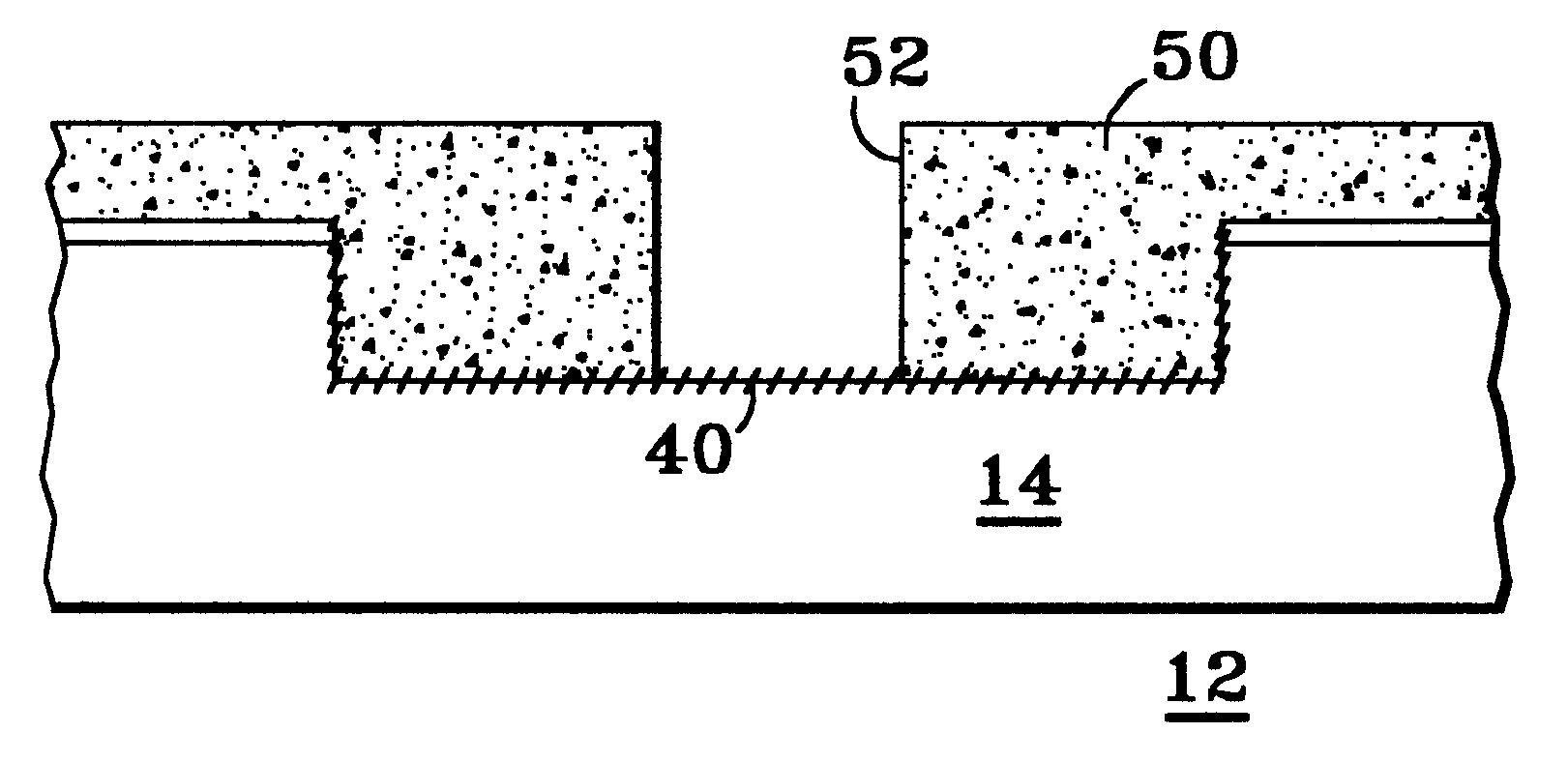
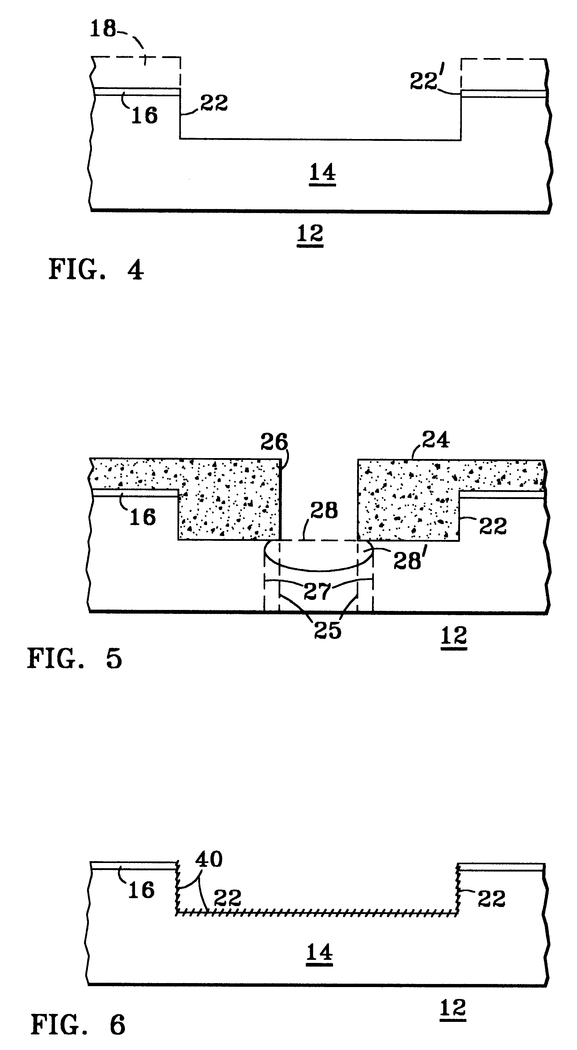
Referring now to FIG. 3, there is shown in cross-section, an early stage in dual Damascene processing to produce conductors at a surface of structure 10 including...
PUM
 Abstract
Description
Claims
Application Information
 - R&D Engineer
- R&D Manager
- IP Professional
- Industry Leading Data Capabilities
- Powerful AI technology
- Patent DNA Extraction
Browse by: Latest US Patents, China's latest patents, Technical Efficacy Thesaurus, Application Domain, Technology Topic.
© 2024 PatSnap. All rights reserved.Legal|Privacy policy|Modern Slavery Act Transparency Statement|Sitemap