Silicon monitor for detection of H2O2 in acid bath

a technology of silicon integrated circuit and monitor, which is applied in the direction of individual semiconductor device testing, semiconductor/solid-state device testing/measurement, instruments, etc., can solve the problems of reducing the production efficiency of microelectronics fabrication, reducing the detection efficiency of microelectronics, and requiring a long time period to determine if contamination was presen

Inactive Publication Date: 2002-03-19
TAIWAN SEMICON MFG CO LTD
View PDF9 Cites 7 Cited by
  • Summary
  • Abstract
  • Description
  • Claims
  • Application Information

AI Technical Summary

Problems solved by technology

Although satisfactory performance is obtained from BOE acid etch bath when proper concentration and temperature are maintained, the use of BOE acid etch bath for etch removal of silicon oxide layers from silicon substrates before metallization is not without problems.
Since hydrogen peroxide may act as an oxidizing agent in acid baths, any excess of this material may itself act as a particular contaminant which could result in yield loss of microelectronics fabrications at Wafer Acceptance Test (WAT) final test.
A lengthy period of time is thus required to determine if contamination was present by yield loss data, due to the large number of processes.

Method used


Image

  • Silicon monitor for detection of H2O2 in acid bath
  • Silicon monitor for detection of H2O2 in acid bath
  • Silicon monitor for detection of H2O2 in acid bath

Examples


Embodiment Construction

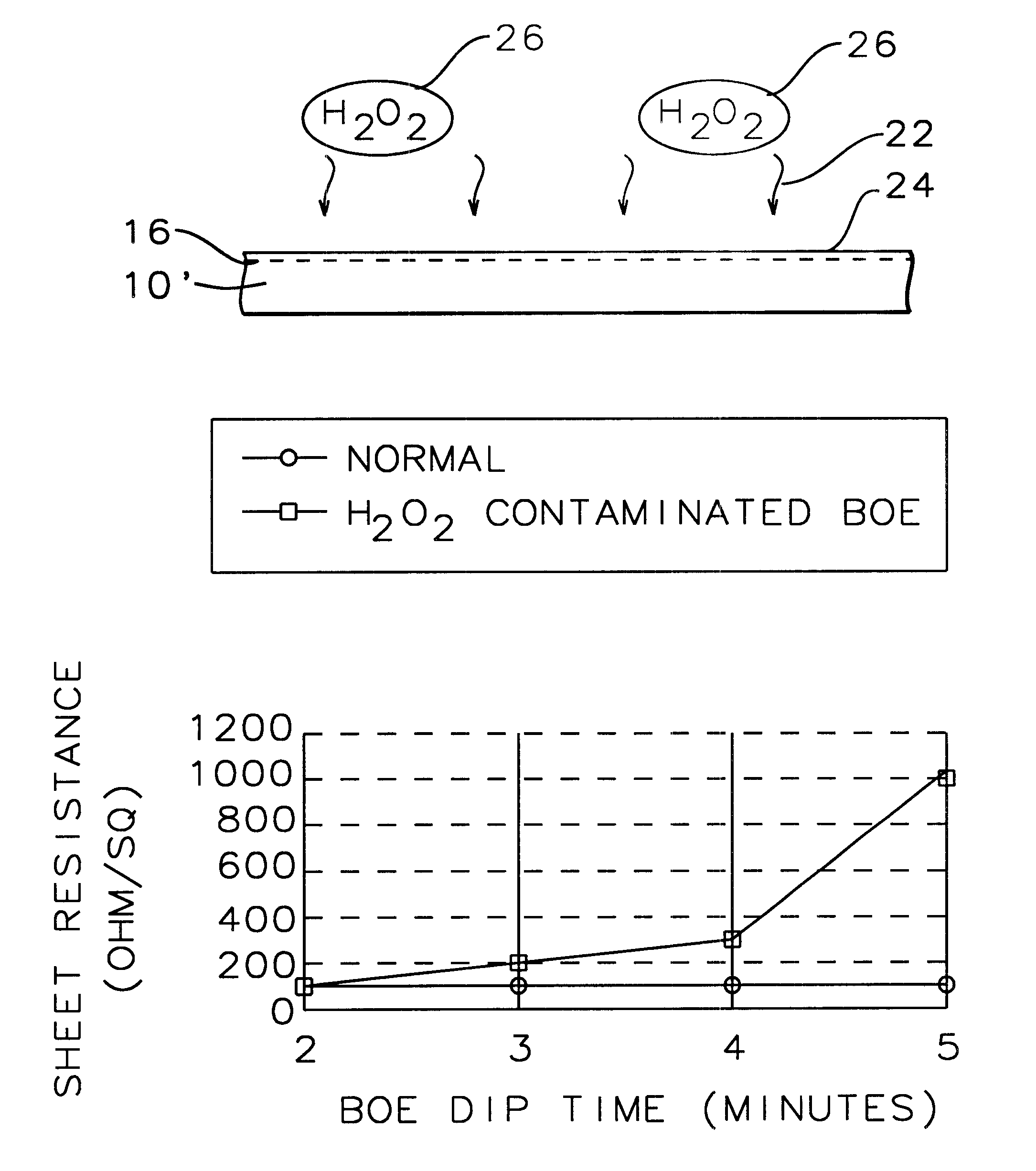
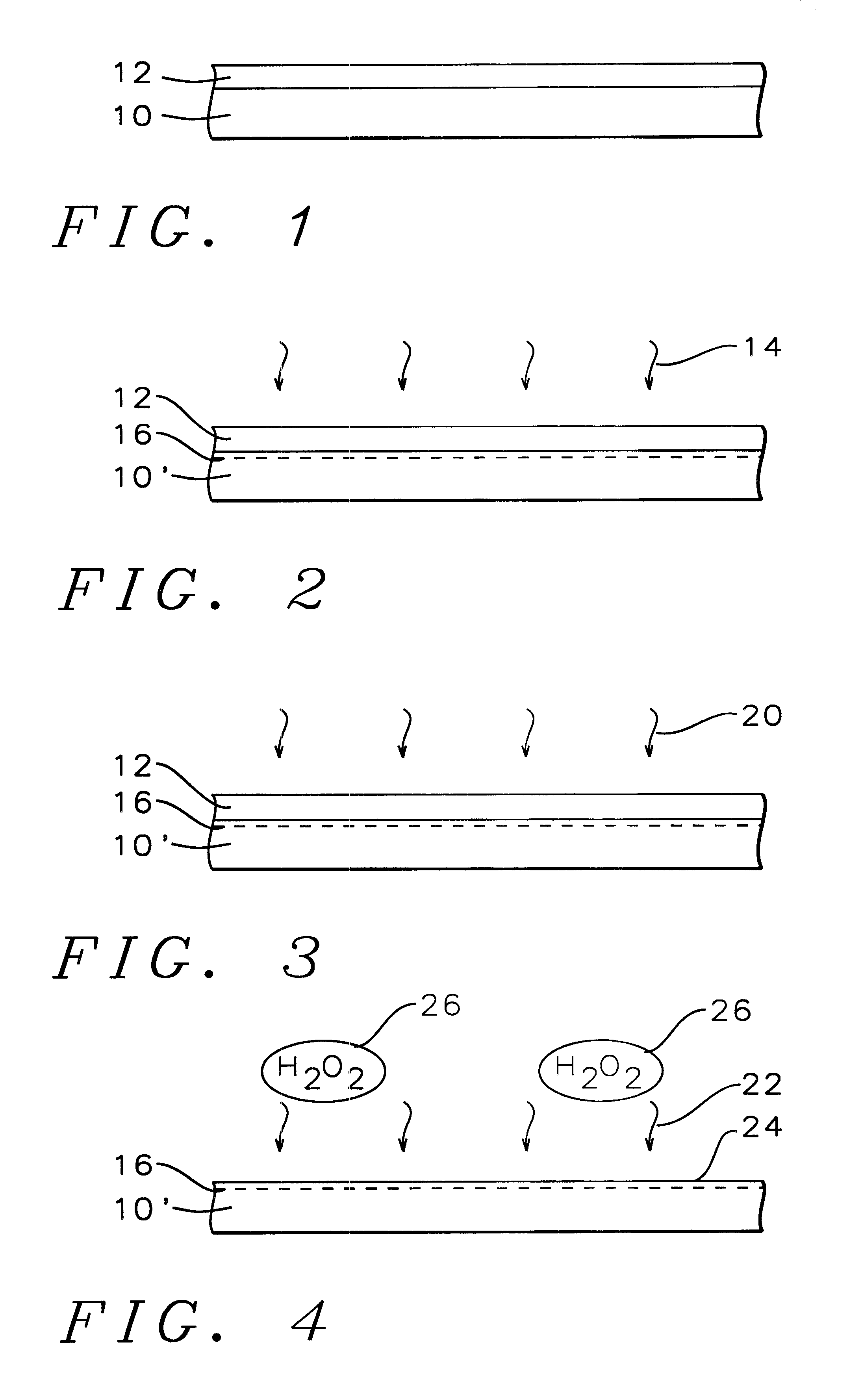
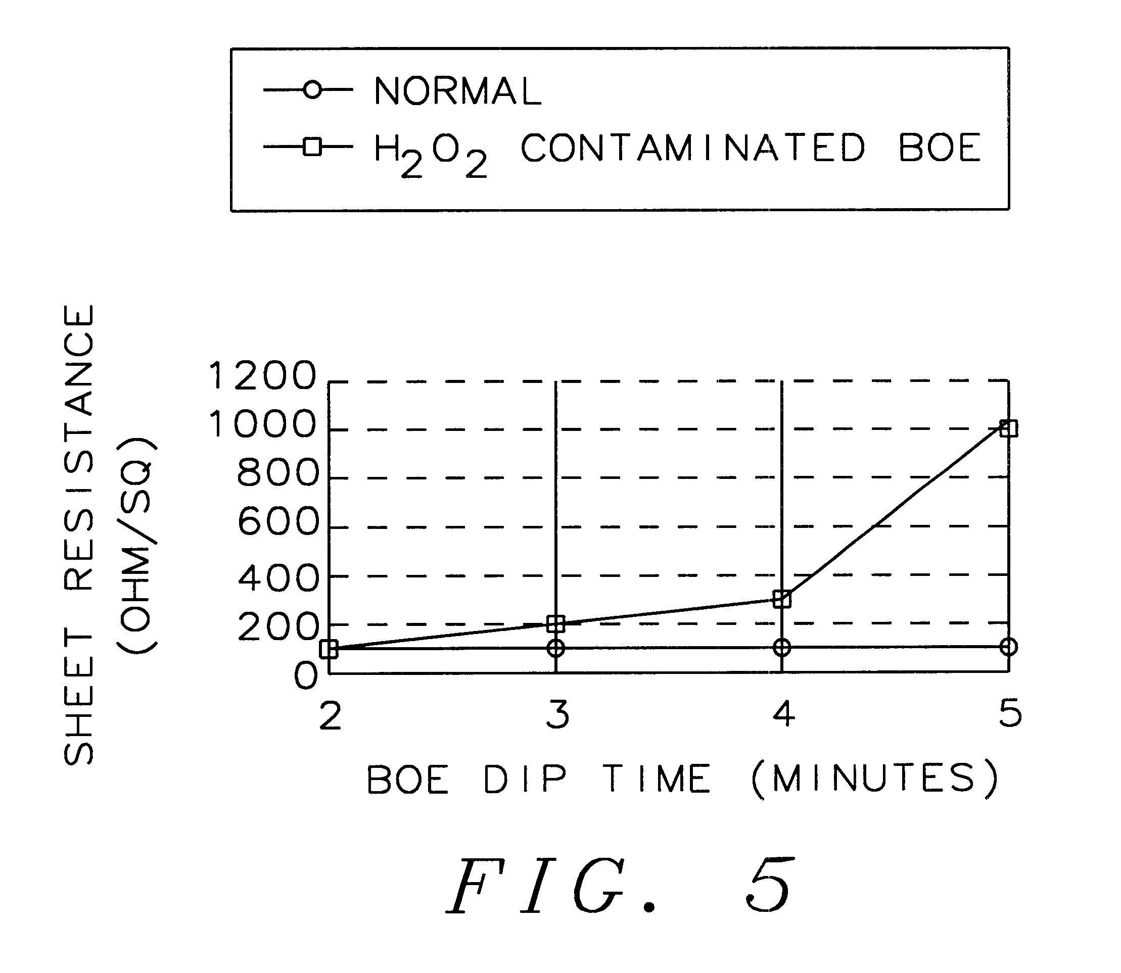
The benefits and advantages of the present invention are exemplified by the experimental data obtained employing silicon monitor substrates determine the effect of hydrogen peroxide contamination in acid etching baths employed to etch the silicon oxide layers from the monitor silicon substrates.

Silicon substrates were prepared according to the following experimental conditions: (1) single crystal (100) silicon substrates with p-type doping from about 15 to about 25 ohm-centimeter resistivity were thermally oxidized in O.sub.2 / HCl at 920 degrees centigrade for 35 minutes to form silicon oxide layers of about 250 angstroms thickness; (2) ion implantation of As.sup.75 ions at 80 keV accelerating potential at a concentration of 1E15 ions / square centimeter; (3) rapid thermal anneal at 1100 degrees centigrade for 10 seconds in nitrogen gas; (4) surface electrical sheet resistance measured to be 122+ / -12 ohm / square; and (5) projected range RP of As.sup.75 ions 388 angstroms, with RP stand...


PUM

PropertyMeasurementUnit
electrical sheet resistanceaaaaaaaaaa
thicknessaaaaaaaaaa
temperatureaaaaaaaaaa

Abstract

A method and means for detection of oxidizing contamination in acid etching baths employed to etch silicon oxide layers from silicon substrates employed in silicon integrated circuit microelectronics fabrications. There is provided a silicon substrate having within a doped region formed employing ion implantation. The silicon substrate is immersed within a buffered oxide etch (BOE) acid bath, wherein the presence of an oxidizing contaminant correlates with an increase in the resistance of the doped region upon the removal of any silicon oxide layer on the silicon surface.

Description

1. Field of the InventionThe invention relates to the field of manufacture of microelectronics fabrications. More particularly the invention relates to the field of monitoring and detecting contamination in silicon integrated circuit microelectronics fabrication processes.2. Description of the Related ArtFabrication of silicon integrated circuit microelectronics devices requires the employment of various chemical processes. A typical microelectronics fabrication is composed of many different materials laminated together, some of which are patterned employing masking techniques and subtractive etching methods employing both wet and dry chemical environments. Of particular interest are chemical systems for etching silicon containing dielectric layers in a controlled fashion. Silicon oxide layers, for example, may often be required to be removed by etching from silicon substrates at a known rate and without deleterious effects on the silicon substrate.One of the principal factors invol...

Claims


Application Information

Patent Timeline
Patent Type & Authority Patents(United States)
IPC IPC(8): G01N27/04
CPCG01N27/041
Inventor YOO, HUI-JUWU, SZU-ANLIN, CHENG-KUNJENQ, SHIOW-JYE
Owner TAIWAN SEMICON MFG CO LTD
Why Eureka
Try Eureka