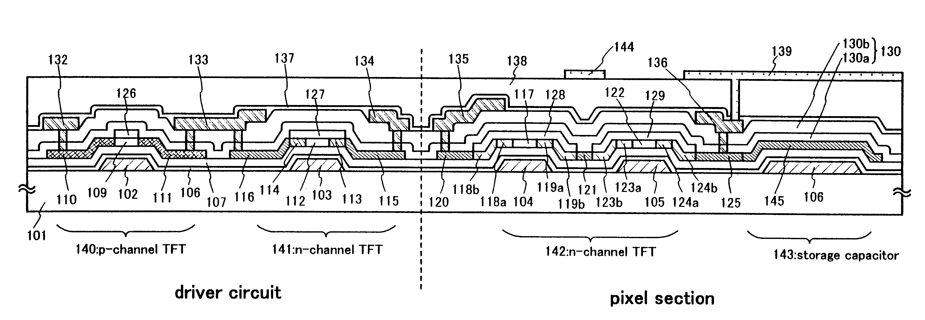
Electro-optical devices in which pixel section and the driver circuit are disposed over the same substrate
a driver circuit and optical technology, applied in the field of semiconductors, can solve the problems of not always the same, not resistant to degradation, and the likelihood of high off current in the crystalline silicon
- Summary
- Abstract
- Description
- Claims
- Application Information
AI Technical Summary
Problems solved by technology
Method used
Image

Examples
embodiments
Embodiment 1
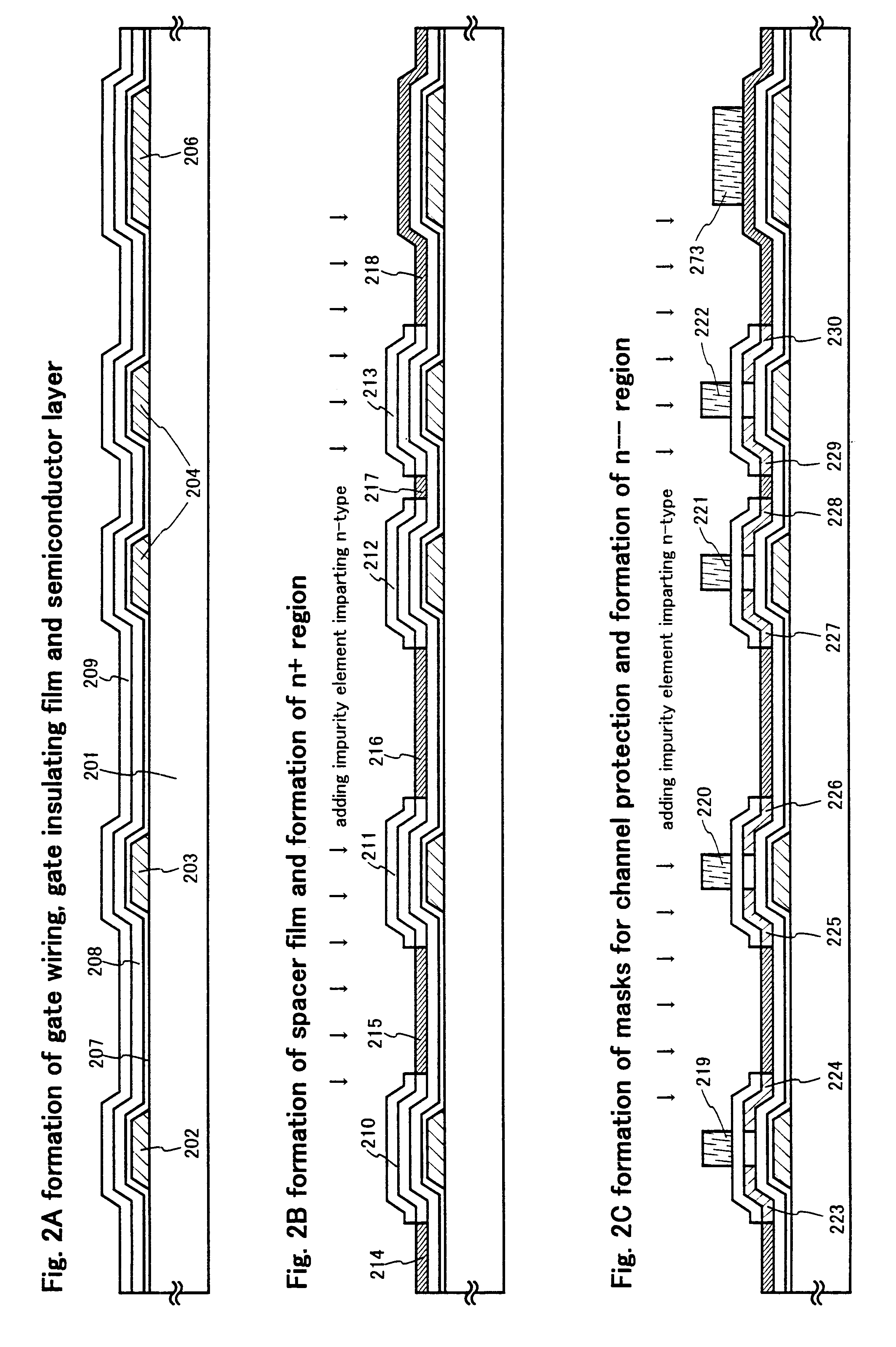
An embodiment of the present invention is described by using FIGS. 2A to 4. A method for manufacturing TFTs of the pixel section and the driver circuit provided in its peripheral are described in detail by following the steps.
(Formation of Gate Electrode, Gate Insulating Film and Semiconductor Layer: FIG. 2A)
In FIG. 2A, a low alkali glass substrate or a quartz substrate was used for the substrate 201. An underlayer film such as a silicon oxide film, silicon nitride film or silicon nitride oxide film may be formed on the surface of the substrate 201 on which TFTs are formed. (not shown)
The gate electrodes 202 to 204 are formed by depositing a film by a publicly known deposition method such as sputtering or vacuum evaporation etc. using an element selected from Ta, Ti, W and Mo or a material whose main component are one of these elements, and then forming patterns by etching to have tapered edge. For instance, a desirable shape can be formed when a Ta film was formed into ...
embodiment 2
A case of simultaneously manufacturing TFTs of a pixel section and a driver circuit disposed in its peripheral by a different method from embodiment 1 is described in Embodiment 2 by using FIGS. 5A to 7B.
First in the similar way to Embodiment 1, gate electrodes 302 to 304, gate wiring (not shown), capacitance wiring 306, gate insulating film formed by double layered structure 307 and 308, and crystalline silicon film 309 are formed over a substrate 301.
A first spacer film comprising a silicon oxide film or a silicon nitride film is formed on the crystalline silicon film 309. Further, a second spacer film is laminated thereon. This film comprises an Al film in order that a selective patterning with the spacer film and the crystalline silicon film is easily performed in the later step, and the thickness is set at 150 nm. Resist masks 310 to 313 are then formed by a publicly known patterning technique, and first spacers 314, 316, 318 and 320, and second spacers 315, 317, 319 and 321 ar...
embodiment 3
An example of other structure of TFTs of pixel section and the driver circuit is described in the present embodiment by using FIGS. 8A to 9. A substrate of the condition of FIG. 5C is formed according to Embodiment 2.
Impurity regions (n.sup.-) 401 to 408 are formed by adding phosphorus (P) into the crystalline silicon film underneath by ion doping interposing the first spacer film. The phosphorus (P) concentration for these regions are set to be 6.times.10.sup.21 cm.sup.-3. A second spacer film functioned here as a mask, and phosphorus (P) is not added to the region where it overlapped with a first spacer film. When ion doping is used, such impurity element doping can be easily performed by properly setting the acceleration voltage. (FIG. 8A)
A process for adding impurity element imparting p-type is then performed into the source region and the drain region of the p-channel TFT of the driver circuit. A new resist mask 409 is formed on the second spacer film 327, and first spacer film...
PUM
 Abstract
Description
Claims
Application Information
 - Generate Ideas
- Intellectual Property
- Life Sciences
- Materials
- Tech Scout
- Unparalleled Data Quality
- Higher Quality Content
- 60% Fewer Hallucinations
Browse by: Latest US Patents, China's latest patents, Technical Efficacy Thesaurus, Application Domain, Technology Topic, Popular Technical Reports.
© 2025 PatSnap. All rights reserved.Legal|Privacy policy|Modern Slavery Act Transparency Statement|Sitemap|About US| Contact US: help@patsnap.com