Semiconductor device and method for manufacturing semiconductor device

a semiconductor and semiconductor technology, applied in the direction of cable/conductor manufacture, electric devices, decorative surface effects, etc., can solve the problems of reducing the resolution occurring during the photolithography step, increasing the degree of integration and the film thickness of the insulating layer, and increasing the resolution

Inactive Publication Date: 2002-04-09
LAPIS SEMICON CO LTD
View PDF6 Cites 21 Cited by
  • Summary
  • Abstract
  • Description
  • Claims
  • Application Information

AI Technical Summary

Problems solved by technology

In contrast, a conventional photoresist mask, which necessitates that the thickness of the photoresist be set to a large value to open deep contact hole since the selection ratio relative to the photoresist (the etching rate ratio of the photoresist / polysilicon) cannot be set large enough, presents problems such as a reduction in resolution occurring during the photolithography step due to the increase in the film thickness.
However, the method for manufacturing a semiconductor device in the prior art described above poses the following problems as the degree of integration and the film thickness of the insulating layers increase.
When the film thickness of an insulating layer increases, it naturally results in an increase in the length of time required for etching to form contact hole.
If a wiring layer is present in the vicinity of a contact hole under these circumstances, the margin between the patterns is reduced by the increase in the diameter of the contact hole, and when the wiring layer to be connected to the contact hole is formed in a subsequent step, a shorting defect may occur between the wiring layer and the electrode provided at the contact hole.
(2) Shape defects caused by a higher aspect ratio.
In order to solve these problems, a high-density, low-pressure plasma must be generated, which necessitates installation of an expensive apparatus.

Method used


Image

  • Semiconductor device and method for manufacturing semiconductor device
  • Semiconductor device and method for manufacturing semiconductor device
  • Semiconductor device and method for manufacturing semiconductor device

Examples


first embodiment

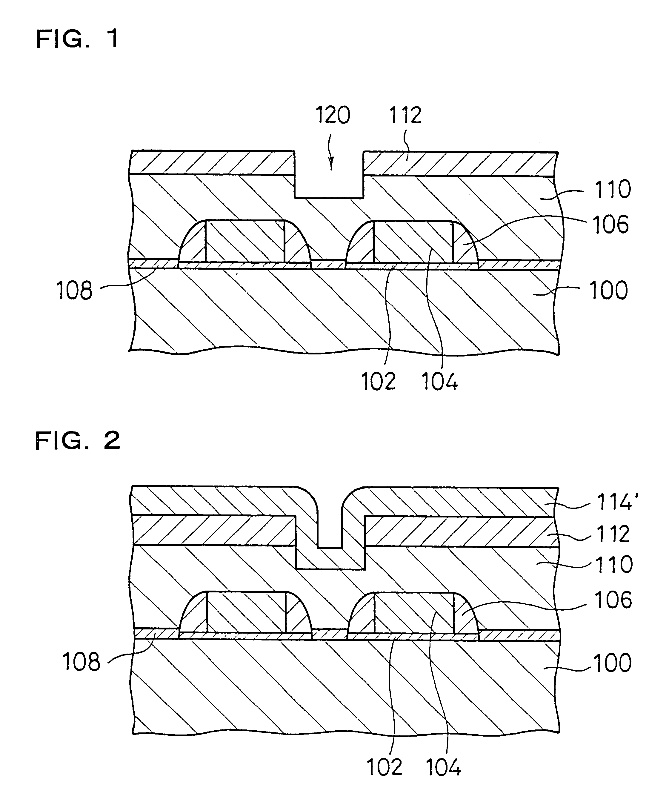
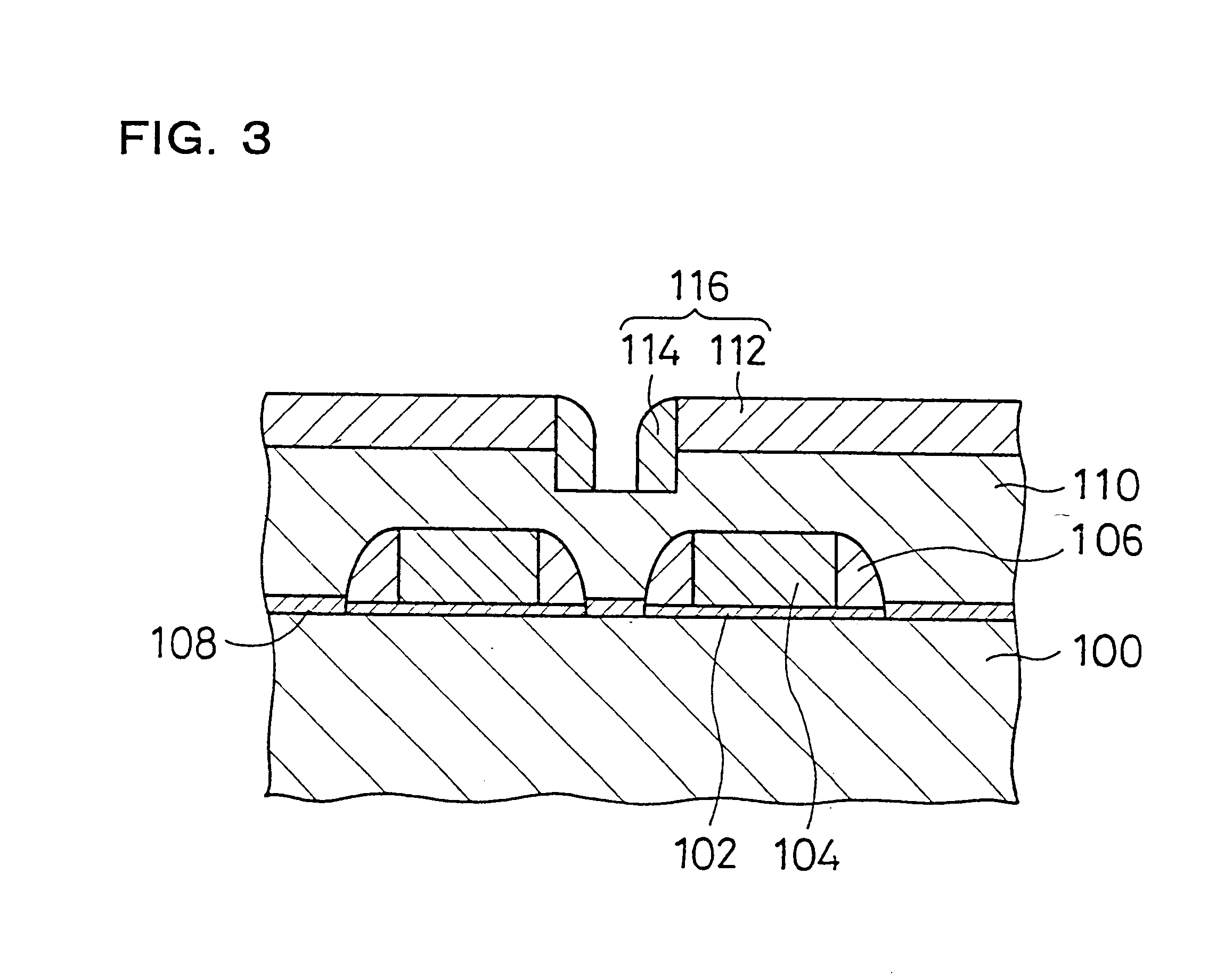
First, the first embodiment is explained in reference to FIGS. 1.about.5. It is to be noted that FIGS. 1.about.5 mainly illustrate the steps taken in the method for manufacturing a semiconductor device in this embodiment.

The method for manufacturing a semiconductor device in the embodiment may be primarily divided into four steps, i.e., an element formation step, an insulating layer formation step, a mask formation step, and a contact hole formation step.

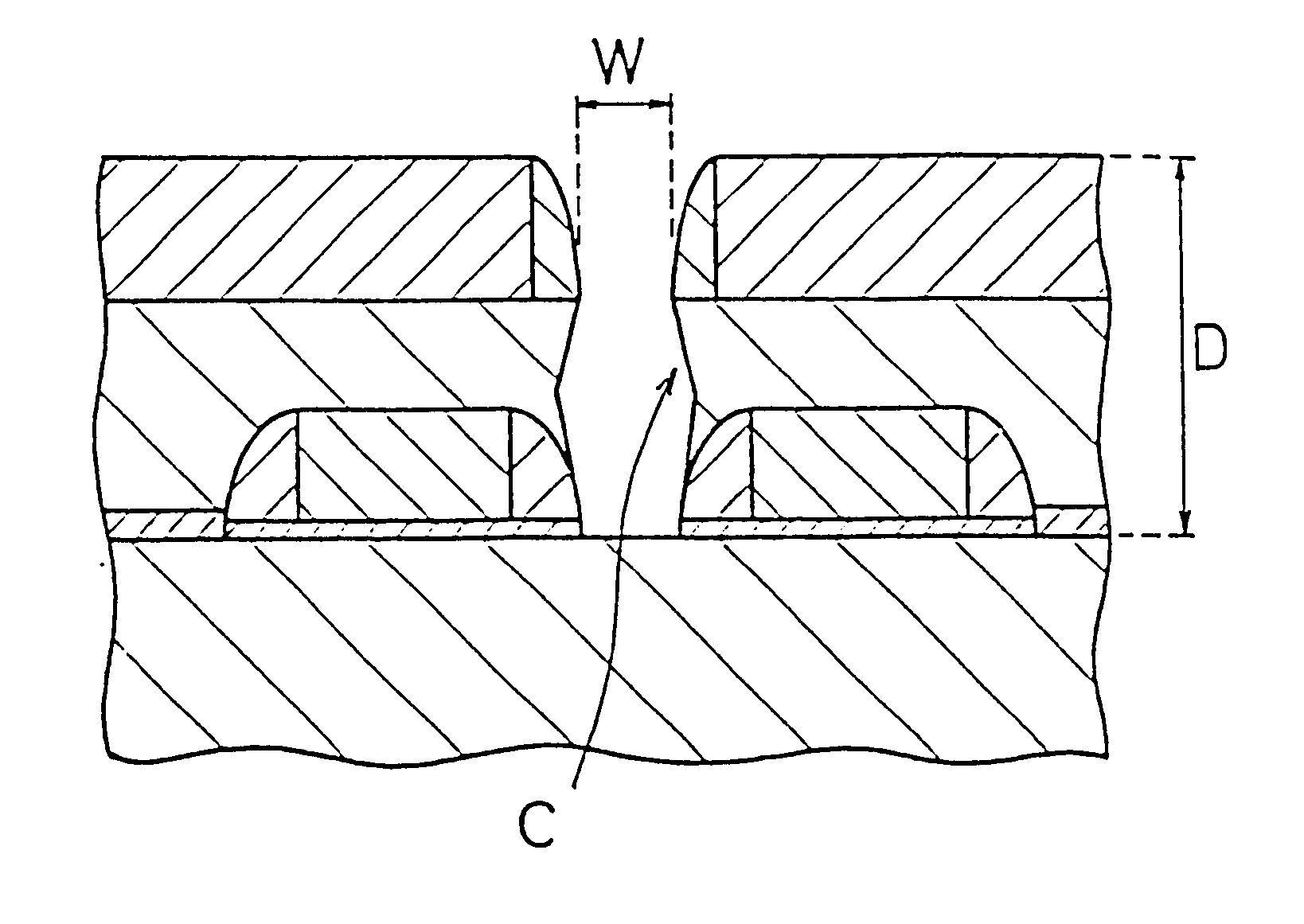
As illustrated in FIG. 1, during the element formation step, a specific element active area is first formed at a silicon substrate 100 which corresponds to the semiconductor substrate. Next, gate oxide film 102 is grown with a specific pattern at the front surface of the silicon substrate 100. Then , polysilicon gates 104 are grown on the gate oxide film 102 to form a gate pattern. Next, a CVD silicon oxide film 106 is grown at side walls of the polysilicon gates 104 to form a side wall spacer pattern. Then, a silicon oxide film 108...

second embodiment

Next, the second embodiment is explained mainly in reference to FIGS. 6.about.9.

In the method for manufacturing a semiconductor device in this embodiment, first, element active areas are formed on a silicon substrate 200, silicon oxide film 202 is grown and a pattern of polysilicon gates 204 constituted of polysilicon is formed as illustrated in FIG. 6. Next, side wall spacers 206 are formed at side walls of the polysilicon gates 204 to form a side wall spacer pattern, then a silicon oxide film 208 is formed at exposed portions of the silicon substrate 200 and specific diffusion layers are formed at the silicon substrate 200 through impurity ion implantation (the diffusion layers are not shown).

Next, a first BPSG film 210a is deposited over the entire surface and is planarized through hot flow, and then a silicon nitride film 220, which corresponds to an etching stop layer is deposited. Then, a second BPSG film 210b is deposited and planarized through hot flow. After this, a polysil...

third embodiment

Next, the third embodiment is explained in reference to FIGS. 10.about.13.

In this embodiment, first, specific element active areas are formed on a silicon substrate 300, a gate oxide film 302 is grown and a pattern of polysilicon gates 304 constituted of polysilicon is formed as illustrated in FIG. 10. After forming side wall spacers 306 at the side walls of the polysilicon gates 304, a silicon oxide film 308 is formed at the exposed portion of the silicon substrate 300 and a specific diffusion layer is formed on the silicon substrate 300 through impurity ion implantation (the diffusion layer is not shown).

Next, a BPSG film 310 is deposited over the entire surface and is planarized through hot flow, and after this, a polysilicon film 312 to constitute a first layer and a silicon nitride film 320 to constitute a second layer are sequentially deposited. Then, through conventional photolithography and etching processes, a preparatory hole 322 which constitutes an initial preparatory ho...


PUM

PropertyMeasurementUnit
diameteraaaaaaaaaa
specific thicknessaaaaaaaaaa
specific depthaaaaaaaaaa

Abstract

In the method for manufacturing a semiconductor device according to the present invention, after forming a BPSG film 110 on a silicon substrate 100, a preparatory hole 120 that reaches a specific depth and has a larger diameter than a contact hole 118 is formed at a position where the contact hole 118 (see FIG. 4) is to be formed at the BPSG film 110. Thus, polysilicon side walls 114 (see FIG. 4) formed at side portions of a polysilicon film 112 (see FIG. 4) are also formed at the side walls of the preparatory hole 120. As a result, the contact hole 118 (see FIG. 4) free of shape defects can be formed by using an etching mask 116 (see FIG. 4) constituted of the polysilicon film 112 and the polysilicon side walls 114. This structure prevents defects related to the shape of the hole and reduces electrical defects such as shorting.

Description

1. Field of the InventionThe present invention relates to a semiconductor device and a method for manufacturing a semiconductor device.2. Description of the Background ArtIn response to the need for miniaturization and higher integration of semiconductor devices, great progress has been made in semiconductor micro-machining technology in recent years. This, in turn, has resulted in practical semiconductor devices having a multi-layer structure achieved by sequentially laminating a plurality of substrates upon which electrical elements are formed alternately with insulating layers. In such a semiconductor device having a multilayer structure, power is normally supplied to the individual electrical elements via through holes which are referred to as contact hole formed at the insulating layers. The contact hole is formed through etching and for this purpose an etching mask is formed through patterning on the front surface of a roughly planar insulating layer in the prior art.In additi...

Claims


Application Information

Patent Timeline
Patent Type & Authority Patents(United States)
IPC IPC(8): H01L21/70H01L21/4763H01L21/768H01L21/02H01L21/3065H01L21/3213H01L21/302
CPCH01L21/76816
Inventor HORIO, TAKUJI
Owner LAPIS SEMICON CO LTD
Why Eureka
Try Eureka