Thermoresistance adhesive and semiconductor device using the same

a technology of adhesive and semiconductor, applied in semiconductor devices, solid-state devices, basic electric elements, etc., can solve the problems of reducing the rate of the sealer used in such devices, hardly being able to provide both secure bonding and film strength, and achieving the effect of sufficient adhesiveness

Inactive Publication Date: 2002-04-16
HITACHI CHEM CO LTD
View PDF11 Cites 29 Cited by
  • Summary
  • Abstract
  • Description
  • Claims
  • Application Information

AI Technical Summary

Benefits of technology

An object of the present invention is to solve these problems and to provide a thermoresistance adhesive which is capable of providing secure bonding (especially heat bonding) of a chip and a lead frame and also has sufficient adhesiveness to the sealer to prevent package cracking in solder reflowing, a solution of such a thermoresistance adhesive, and a semiconductor chip having a thermoresistance adhesive layer, lead frame having a thermoresistance adhesive layer, a film having a thermoresistance adhesive layer, and a semiconductor device.
The semiconductor chip used in the present invention is preferably the one having a thermoresistance adhesive layer obtained by attaching a perforated adhesive-applied metal or resin film with a Young's modulus of 2 GPa or greater to a semiconductor wafer, injecting said heat-resistant resin or heat-resistant resin composition into the holes in the film by a dispenser or other means, squeegeing the film, then peeling the film after drying if necessary, and dicing it. According to this method, a thermoresistance adhesive layer can be formed with minimized risk of chip damage (such as disconnection of electric circuits).

Problems solved by technology

Recently, with advancement of miniaturization of semiconductor devices, the proportion of the chips in the semiconductor devices has increased while the rate of the sealer used in such devices has decreased, and this situation is blamed for the frequent occurrence of package cracking, a phenomenon caused as the moisture absorbed in the thermoresistance adhesive or sealer is vaporized and expanded by the heat such as generated from soldering treatment (solder reflowing).
With the conventional adhesives, however, it has been hardly possible to provide both secure bonding (especially heat bonding) of the chip and lead frame and enough adhesiveness to the sealer to prevent package cracking in solder reflowing.
In most of the hitherto developed thermoresistance resin pastes, fine silica particles or non-soluble fine polyimide particles are used as the filler for affording the thixotropic properties, so that these resin pastes involve the problem that many voids or air cells are formed at the filler interface during heat drying to lower the film strength.
According to this method, however, dust or other ionic impurities tend to mix in the thermoresistance resin paste from the mixer and / or the mixing atmosphere, so that this technique was unsuited for such uses as production of semiconductor elements and also unsatisfactory in terms of productivity.
Further, since the specific organic filler (soluble filler) is generally produced by a reprecipitation method in which a dilute polyimide resin solution is supplied into a poor solvent of the polyimide resin and the precipitated fine solid particles are recovered, the process was complicated and low in productivity.

Method used


Image

  • Thermoresistance adhesive and semiconductor device using the same
  • Thermoresistance adhesive and semiconductor device using the same
  • Thermoresistance adhesive and semiconductor device using the same

Examples


example 2

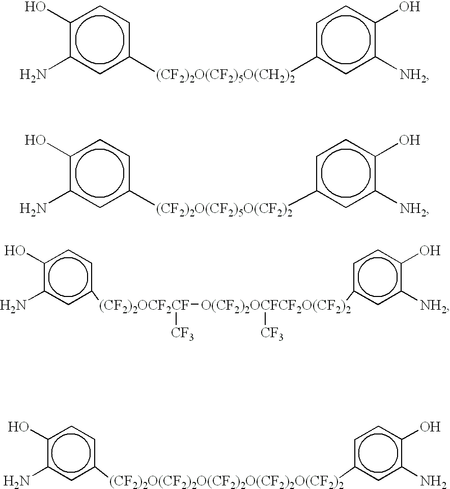
To a 1,000 ml four-necked flask equipped with a stirrer, a thermometer, a nitrogen gas inlet pipe and a condenser provided with an oil / water separator, 65.69 g (0.16 mol) of BAPP, 143.22 g (0.40 mol) of bis(3,4-dicarboxylphenyl)sulfone dianhydride (hereinafter abbreviated to DSDA), 38.84 g (0.20 mol) of isophthalic acid dihydrazide (hereinafter abbreviated to IPDH), 9.93 g (0.04 mol) of 1,3-bis(aminopropyl)tetramethyldisiloxane and 478 g of BL were supplied while blowing nitrogen gas through the solution. After one-hour reaction at 50 to 60.degree. C. with stirring, the temperature was raised to 195.degree. C. and the reaction was continued at this temperature for 6 hours. Water generated in the course of the reaction was rapidly removed out of the reaction system. The resulting solution was diluted with BL to obtain a polyamide-imide resin solution with a resin concentration of 30% by weight.

To a 1,000-ml four-necked flask equipped with a stirrer, a thermometer, a nitrogen gas inle...

example 3

To a 1,000-ml four-necked flask equipped with a stirrer, a thermometer, a nitrogen gas inlet pipe and a condenser with an oil / water separator, 102.64 g (0.25 mol) of BAPP, 127.83 g (0.357 mol) of DSDA, 23.13 g (0.107 mol) of 2,2-bis(4-hydroxy-3-aminophenyl)propane (hereinafter abbreviated to HAB) and 380 g of N-methylpyrrolidone (hereinafter abbreviated to NMP) were supplied while blowing nitrogen gas through the solution. After one-hour reaction at 50 to 60.degree. C. with stirring, the temperature was raised to 195.degree. C. and the reaction was continued at this temperature for 5 hours. Water generated in the course of the reaction was rapidly removed out of the reaction system. The resulting solution was diluted with NMP to obtain a polyimide resin solution with a resin concentration of 40% by weight.

To 200 g of this polyimide resin solution was added 8 g of .gamma.-glycidoxypropyltrimethoxysilane (hereinafter abbreviated to GPS), followed by mixing well at room temperature to ...

example 4

To a 1,000-ml four-necked flask equipped with a stirrer, a thermometer, a nitrogen gas inlet pipe and a condenser provided with an oil / water separator, 89.09 g (0.217 mol) of BAPP, 119.59 g (0.334 mol) of DSDA, 42.85 g (0,117 mol) of 2,2-bis(4-hydroxy-3-aminophenyl)hexafluoropropane (hereinafter abbreviated to HAB-6F) and 377 g of BL were supplied while blowing nitrogen gas through the solution. After one-hour reaction at 50 to 60.degree. C. with stirring, the temperature was raised to 195.degree. C. and the reaction was continued at this temperature for 5 hours. Water generated in the course of the reaction was rapidly removed out of the reaction system. The resulting solution was diluted with BL to obtain a polyimide resin solution with a resin concentration of 40% by weight.

To a 1,000-ml four-necked flask equipped with a stirrer, a thermometer, a nitrogen gas inlet pipe and a condenser, 400 g of the solvent-containing solid polyimide resin for filler obtained in Example 2 (resin ...


PUM

PropertyMeasurementUnit
sizeaaaaaaaaaa
temperatureaaaaaaaaaa

Abstract

A thermoresistance adhesive which does not dissolve in the sealer-composing resins at the sealer molding temperature and is capable of providing a semiconductor chip / lead frame adhesive strength under shear of 1 N / 4 mm2 or greater, and including, for example, amide, imide, ester or ether linkage is suited for use in producing thermoresistance adhesive solutions and thermoresistance resin pastes, and the semiconductor chips, lead frames, films, etc., made by using such an adhesive are suited for providing low-cost semiconductor devices.

Description

The present invention relates to a thermoresistance adhesive, a thermoresistance adhesive solution, a thermoresistance resin paste, a process for the preparation thereof, a semiconductor chip having a thermoresistance adhesive layer, a lead frame having a thermoresistance adhesive layer, a film having a thermoresistance adhesive layer, and a semiconductor device.The resin-sealed semiconductor devices are typically of the structures such as illustrated in FIGS. 1 to 3. A thermoresistance adhesive is used for bonding the inner leads of a lead frame to a semiconductor chip in the semiconductor device of FIG. 1, or bonding the inner leads of a lead frame which doubles as a buffer coat to the chip surface in the semiconductor device of FIG. 2. In an ordinary semiconductor device shown in FIG. 3, the said adhesive is utilized for bonding a lead frame tab (die pad) to the back side of a chip. The structures of the semiconductor devices of the type illustrated in FIGS. 1 and 2 are called le...

Claims


Application Information

Patent Timeline
Patent Type & Authority Patents(United States)
IPC IPC(8): C09J9/00H01L23/48H01L23/495C08L79/08C08J3/24C09J179/08H01L21/52H01L23/29H01L23/31
CPCC09J9/00H01L23/4951H01L2924/01015H01L2224/32014H01L2224/48091H01L2224/48247H01L2224/4826H01L2924/01012H01L2924/01039H01L2924/01057H01L2924/01079H01L2924/3025H01L2924/10253H01L2224/73215H01L2224/32245H01L24/45H01L2224/45147H01L2224/45124H01L2224/45144H01L2924/01021H01L24/48H01L2924/00014H01L2924/00H01L2924/00012H01L2924/181H01L2224/73265C09J2203/326
Inventor SAKATA, TOUICHINISHIZAWA, HIROSHIHIRAI, KEIZOSUZUKI, KENJI
Owner HITACHI CHEM CO LTD
Why Eureka
Try Eureka