Semiconductor device and method for fabricating the same

a technology of semiconductor devices and semiconductor layers, applied in semiconductor devices, electrical equipment, transistors, etc., can solve the problems of difficult control of the thickness of the p.sup.+-type single crystal silicon layer to be electrically connected to the polysilicon for base extended electrodes, the number of process steps and the increase of the fabrication cost, etc., to achieve the effect of reducing the thermal budget after the deposition of the sige layer, reducing the number of steps of the bicmos process

Inactive Publication Date: 2002-06-04
PANASONIC CORP
View PDF8 Cites 69 Cited by
  • Summary
  • Abstract
  • Description
  • Claims
  • Application Information

AI Technical Summary

Benefits of technology

In the method for fabricating a BiCMOS device according to this embodiment, the order in which the processes of forming the bipolar transistor and CMOS blocks are performed is just reverse to the first embodiment. Accordingly, as in the fabricating method of the first embodiment, the number of steps of a BiCMOS process can be reduced and the productivity and throughput can be increased.
Particularly, i

Problems solved by technology

However, where a base layer for a bipolar transistor is formed by the known selective epitaxial growth, the following problems arise.
Firstly, if an insulating film with a thickness (about 140 nm) greater than that of the base layer subjected to the selective epitaxial growth is used, problems often arise in terms of the yield and productivity.
For example, the type of SiGe epitaxial growth (selective or non-selective growth) and the thickness of a P.sup.+ -type single crystal silicon layer to be electrically connected to the polysilicon for base extended electrode are difficult to contro

Method used


Image

  • Semiconductor device and method for fabricating the same
  • Semiconductor device and method for fabricating the same
  • Semiconductor device and method for fabricating the same

Examples


Embodiment Construction

4

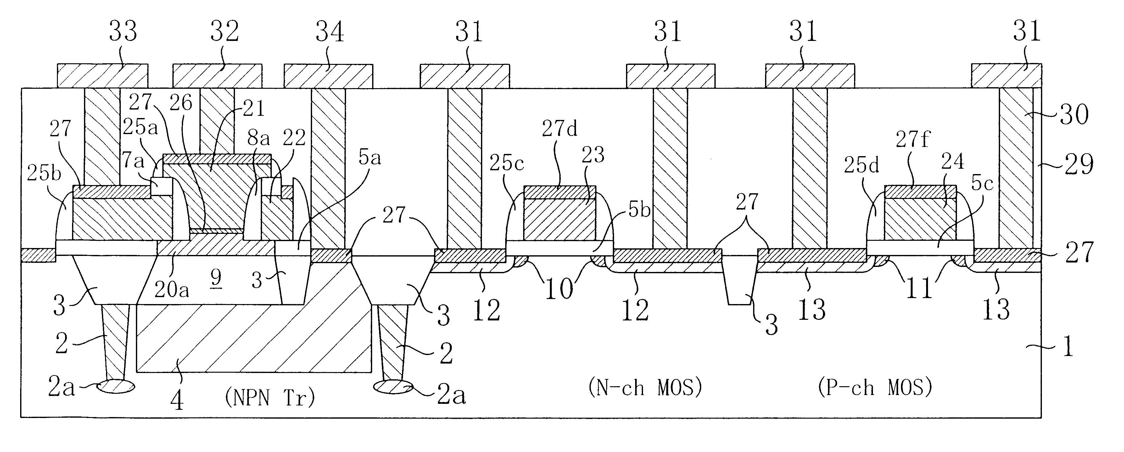
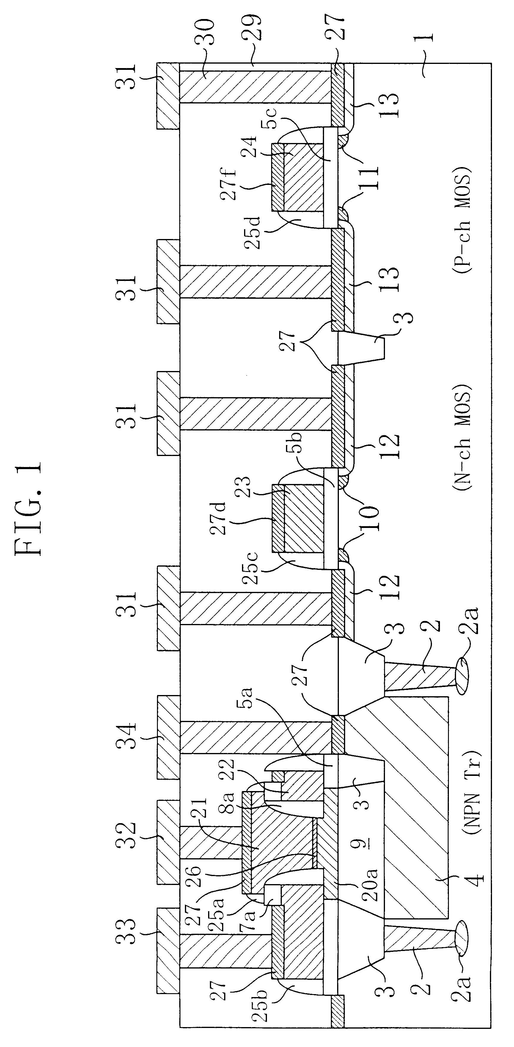
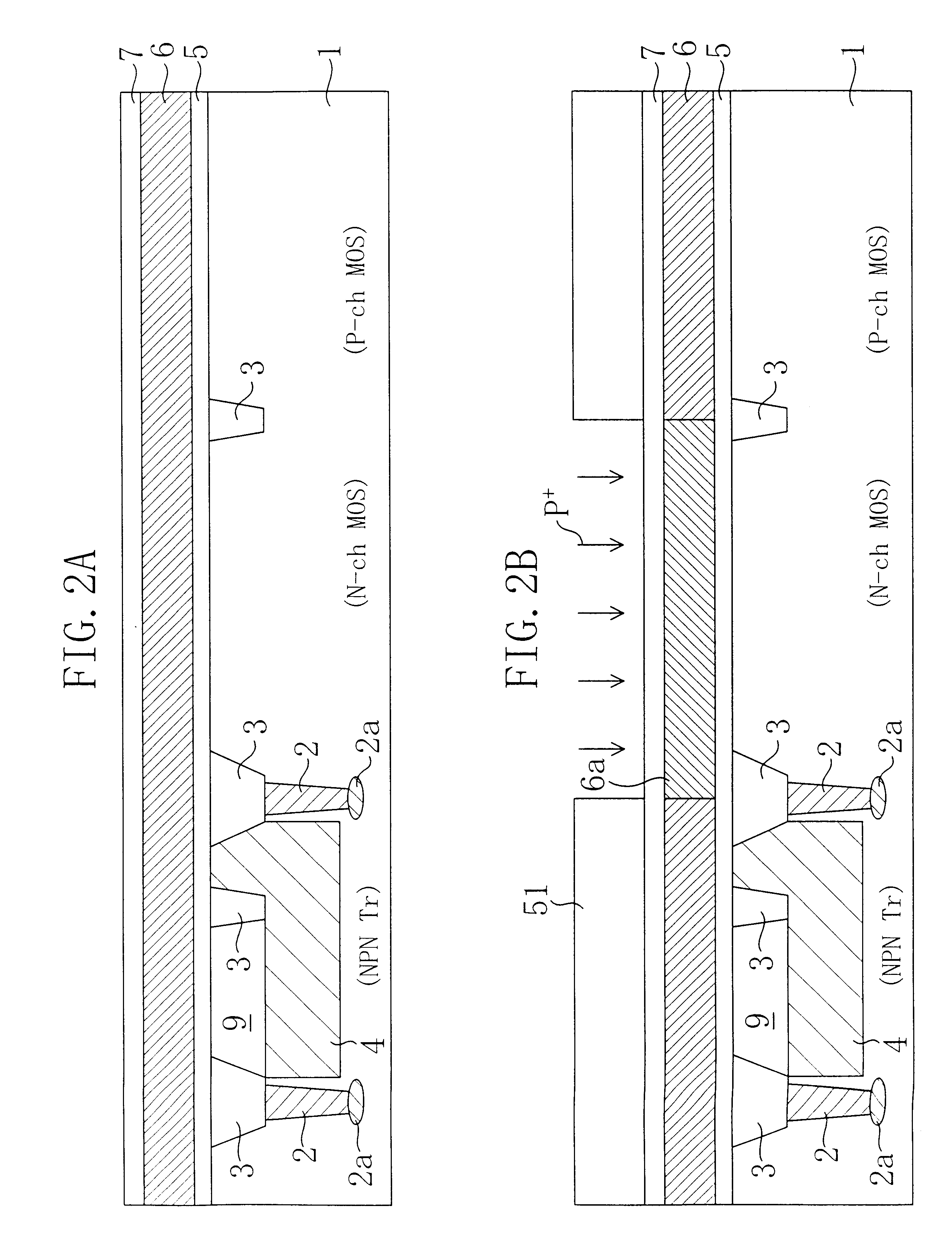
FIG. 18 is a cross-sectional view illustrating a structure for a BiCMOS device according to a modified example of the fourth embodiment. The structure of the BiCMOS device shown in FIG. 18 is basically the same as that of the BiCMOS device of the first embodiment shown in FIG. 1. Accordingly, the same members as the counterparts shown in FIG. 1 are identified by the same reference numerals as those used in FIG. 1 and the description thereof will be omitted herein. This embodiment is the same as the fourth embodiment in that the base layer 41 is made of SiGeC single crystals but different from the fourth embodiment in that the thickness of the base layer 41 is about 20 nm and is thinner than the first insulating film 5a. In this case, the thickness of the first insulating film 5a is about 50 nm, which is considerably thicker than the gate insulating films 5b and 5c with a thickness of 7 nm for the MIS transistor block.

Even in such an embodiment, by adjusting the composition of the S...


PUM


Abstract

In a bipolar transistor block, a base layer (20a) of SiGe single crystals and an emitter layer (26) of almost 100% of Si single crystals are stacked in this order over a collector diffused layer (9). Over both edges of the base layer (20a), a base undercoat insulating film (5a) and base extended electrodes (22) made of polysilicon are provided. The base layer (20a) has a peripheral portion with a thickness equal to that of the base undercoat insulating film (5a) and a center portion thicker than the peripheral portion. The base undercoat insulating film (5a) and gate insulating films (5b and 5c) for a CMOS block are made of the same oxide film. A stress resulting from a difference in thermal expansion coefficient between the SiGe layer as the base layer and the base undercoat insulating film 5a can be reduced, and a highly reliable BiCMOS device is realized.

Description

The present invention relates to a method for fabricating a BiCMOS device: and a structure thereof, and more particularly relates to a BiCMOS device, in which a base layer is formed for a bipolar transistor by a selective epitaxial growth technique.A bipolar transistor has been used as a circuit element with high-speed and high-current characteristics. Particularly, a type of high-performance bipolar transistor is called a "self-aligned base transistor", an example of which is disclosed in U.S. Pat. No. 4,319,932. According to a technique disclosed in this patent, by implanting a dopant through an implantation window, raised sub-collector, intrinsic base and emitter layers are formed.Also, a technique of forming a heterojunction for enhancing the performance of a bipolar transistor is known. To form a heterojunction in a transistor with a silicon substrate for that purpose, a technique of using a material with a bandgap wider than that of Si for a base layer (e.g., GaP, SiC or amorp...

Claims


Application Information

Patent Timeline
IPC IPC(8): H01L21/762H01L21/70H01L21/8249
CPCH01L21/8249H01L21/76237
Inventor OHNISHI, TERUHITOASAI, AKIRATAKAGI, TAKESHISAITOH, TOHRUICHIKAWA, YOHARA, YOSHIHIROYUKI, KOICHIRONOZAWA, KATSUYAKATAYAMA, KOJIKANZAWA, YOSHIHIKO
Owner PANASONIC CORP
Why Eureka
Try Eureka