Method for manufacturing build-up multi-layer printed circuit board by using yag laser

a multi-layer printed circuit board and laser technology, applied in printed circuit assembling, resistive material coating, metallic material coating process, etc., can solve the problems of difficult copper processing, small circuits can be easily formed, thin thickness of circuit conductors,

Inactive Publication Date: 2002-06-18
SAMSUNG ELECTRO MECHANICS CO LTD
View PDF19 Cites 144 Cited by
  • Summary
  • Abstract
  • Description
  • Claims
  • Application Information

AI Technical Summary

Problems solved by technology

Further, in forming the via hole, extremely small diameters are possible, and the thickness of the circuit conductors is very thin, with the result that tiny circuits can be easily formed.
However, in the case of the excimer laser, the processing of the copper is difficult, and therefore, in the pre-stacked board, the copper foil on the organic film-coated foil 14 has to be removed by etching before the hole is formed by means of the excimer laser.
Or only the organic film 15 without the copper foil 14 may be used, but in this case, the pressing for the pre-stacking becomes difficult.
In this case, the organic film-coated copper foil is completely removed by etching, and then, a Cu electroplating is carried out, this being a troublesome task.
Further, in the case where a material RF-4 is used as substitution for the organic film, the use of the excimer laser becomes impossible.
Therefore, the selection of the material for the insulating layer is limited, and the freedom for the drilling depth is lowered, with the result that the density is lowered, Besides, the excimer laser uses toxic gases such as Xe, Cl, XrF, and therefore, a perfect sealing is required.
Therefore, the manufacturing factory may cause an environmental pollution.
As mentioned, however, the conventional method should have a double process, which results in some problems in that the hole process is made in a complicated manner and thereby, the productivity would be decreased.
Moreover, the hole process of a diameter of 100 .mu.m or less is not possible due to the resolution limit of an etch resist, such that a high integrated component packaging density would not be obtained.
At this time, in case of using KMnO.sub.4, the resins on the left and right portions within the interior of the via hole would be undesirably damaged.
However, in this method, in order to form the via hole, the conductive mental layer is partly exposed, and then, a wet etching and laser beams are used, with the result that the process is complicated.
However, the material layer which is highly sensitive to the laser beams is used for the laser drilling, and therefore, a superfluous process step is added.

Method used


Image

  • Method for manufacturing build-up multi-layer printed circuit board by using yag laser
  • Method for manufacturing build-up multi-layer printed circuit board by using yag laser
  • Method for manufacturing build-up multi-layer printed circuit board by using yag laser

Examples


Embodiment Construction

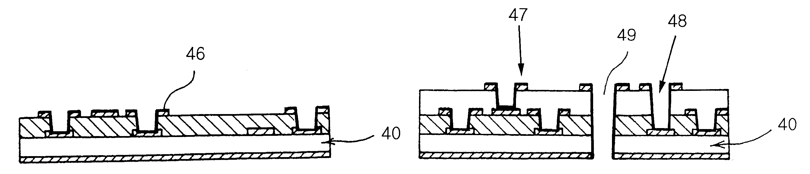
As shown in FIG. 4, a printed pattern 41 was formed on a CCL 40 on which copper foils had been attached on the both faces thereof. Then a black oxide treatment was carried out on the printed pattern. Then, a resin-coated copper foil was stacked on the board 40. The resin-coated copper foil had a transition temperature of about 130.degree. C., and its thickness was 40 .mu.m. Then, heating and pressing was carried out at a pressure of 20-30 kg / cm.sup.2 and at a temperature of 180.degree. C. for 45 minutes or more. Thereafter, ND-YAG laser beams were irradiated to the relevant portion of the board to drill a tapered via hole having a diameter of about 60 .mu.m.

Under this condition, the operating conditions for the YAG laser were as follows. That is, the laser pulse repetition rate was 0.785 KHz, the distance between the laser beams(bite doze) was 6.67 .mu.m, the displacing velocity of the laser beams was 5,235 mm / sec, the number of passes was 1 pass, the effective spot size of the hole...


PUM

PropertyMeasurementUnit
thicknessaaaaaaaaaa
diameteraaaaaaaaaa
diameteraaaaaaaaaa

Abstract

A method for manufacturing a build-up multi-layer printed circuit board is disclosed in which a YAG laser is used upon the formation of a via hole in the multi-layer printed circuit board, such that it can have the following advantages: the manufacturing process would become simple; the component packaging density and freedom for the design of the board would be improved; and a high speed of signal process would be ensured. The method for manufacturing a build-up multi-layer printed circuit board includes the steps of: forming a first printed circuit pattern on a copper clad laminate (CCL) by applying a general photo-etching process, the CCL having a copper foil on the one face thereof; stacking a resin-coated (on one face) copper foil (RCC) on the CCL with the first printed circuit pattern formed thereon, and heating and pressing this structure; irradiating a YAG laser to the board with said RCC stacked so as to form a via hole at a predetermined position by removing said RCC; carrying out an electroless and electro copper plating on the board with the via hole formed therein to form a plated layer; and forming a second printed circuit pattern on said plated layer to electrically connect the layers on which the first and second printed circuit patterns are formed.

Description

1. Field of the InventionThe present invention relates to a method for manufacturing a multi-layer printed circuit board for use in computers, VTR, portable telephones and the like. More particularly, the present invention relates to a method for manufacturing a build-up multi-layer printed circuit board in which an yttrium aluminum garnet (hereinafter, referred to as "YAG") laser is used upon the formation of a via hole in the multi-layer printed circuit board, such that it can have the following advantages: the manufacturing process would become simple; the component packaging density and freedom for the design of the board would be improved; and a high speed of signal process would be ensured.2. Description of the Prior ArtIn the midst of the progress of the electronic components and the component installation technique, the printed circuit board was devised. Since that time, studies have been briskly carried out to make the printed circuit board highly dense. Particularly, the m...

Claims


Application Information

Patent Timeline
Patent Type & Authority Patents(United States)
IPC IPC(8): H05K3/46H05K3/00
CPCH05K3/0038H05K3/4652H05K3/0035Y10T29/49165H05K2201/09518Y10T29/49126Y10T29/49155H05K2201/0358
Inventor SHIN, DONGPARK, KEON YANGSHIN, YOUNG HWANSUN, BYUNG KOOKJOUNG, JAE HEUN
Owner SAMSUNG ELECTRO MECHANICS CO LTD
Why Eureka
Try Eureka