However, with the further
miniaturization of the circuit pattern, it has been a concern that the resolution of the light is approaching its limit.
However, in so-called direct-writing method where the writing is performed by scanning very fine electron beam, it takes a very long time to form a large-area or large-size pattern, that is, the
throughput (a
processing rate per unit time) is low.
In general, it is considered that the clear pattern is caused by an error made at the time when the pattern is projected onto a membrane (at the time of the
resist-pattern writing), so that the portion where the
resist pattern is missing becomes itself a clear defect.
On the other hand, a opaque defect is the electron
beam scattering material which has remained in unwanted areas due to the fact that such foreign materials or the like, for example one that could become an
etching mask, adheres to the
resist pattern.
However, there is a problem that after the milling is once performed the material adheres again to a portion of the pattern.
Moreover, though the gas to be supplied has a low
etching capacity, the gas corrodes the material to be etched.
Thus it is difficult to appropriately control the shape of a cross section of a portion to be processed.
(1) Since the reduction projection lithography method using an electron beam concerns a technology forming a pattern of less than 0.1 .mu.m, it is necessary to form an
electron scattering material pattern of less than 0.4 .mu.m on the
reticle in the event that the
reduction factor is one forth. On the other hand, as the electron beam scattering material requires a thickness of approximately 2 .mu.m, the
aspect ratio of the electron beam scattering material pattern is approximately 5. Since severe specification is required for the size of a portion to be processed in a
reticle and a cross sectional shape thereof, the miniaturization
processing for the
reticle requires an advanced
processing technique as the
aspect ratio increases, thus its processing becomes excessively difficult to carry out.
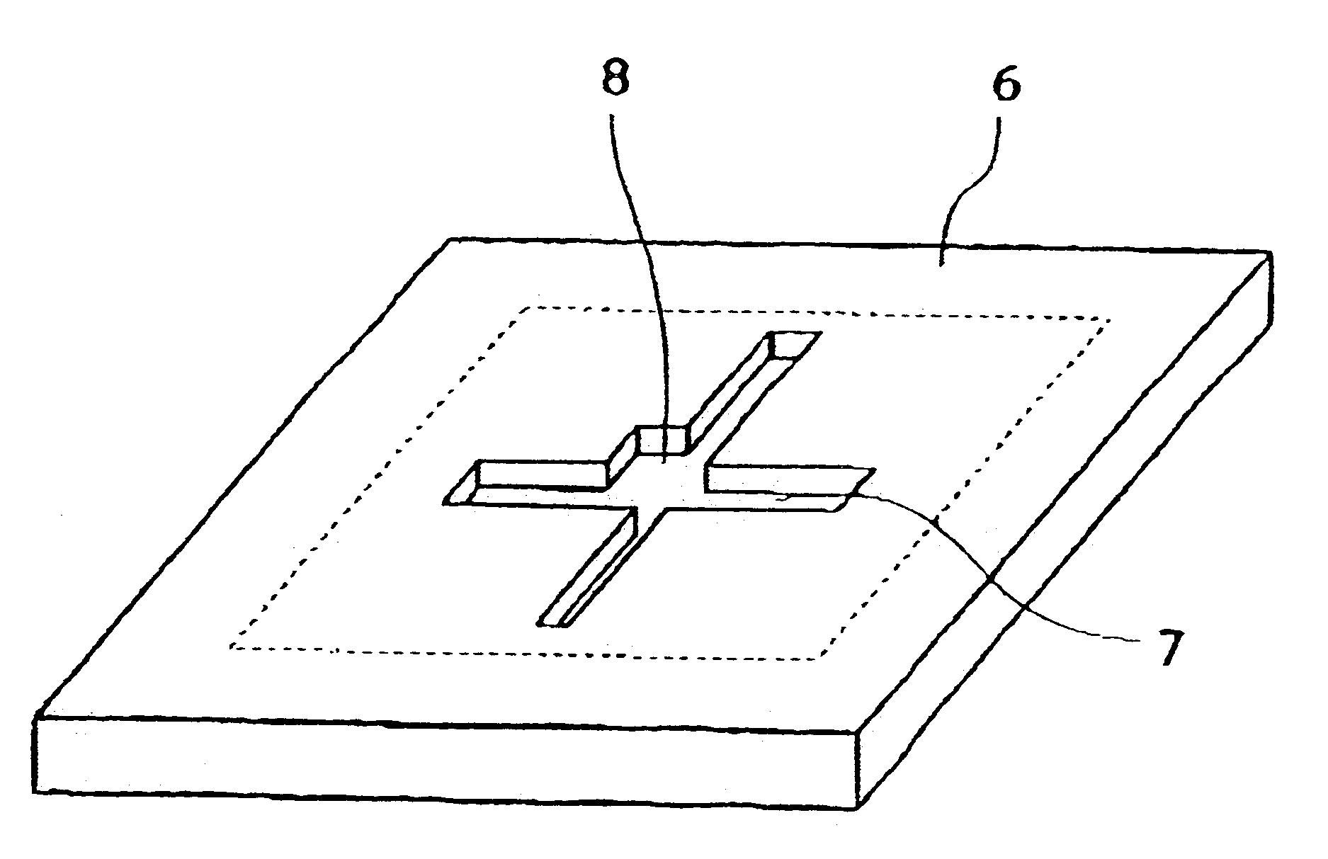
(2) The reticle, or mask, used in reduction projection lithography using an electron beam is constituted by the electron beam scattering material alone, and is of so-called scattering stencil type. Namely, in this scattering stencil type mask, a pattern of an electron beam scattering material is not formed on the substrate which is illuminated by the electron beam, instead, the region which is illuminated by the electron beam is opened, so that the projected pattern is formed and consists of the electron beam scattering material alone. In scattering stencil reticle,
incident beam is usually absorbed by the membrane or substrate but can pass through void, aperture, opening which forms a pattern. In scattering stencil reticle,
incident beam is scattered by the membrane or substrate but can pass through void, aperture, opening which form pattern to be projected. In scattering membrane reticle,
incident beam is scattered by the scatterer on the reticle surface, which forms pattern to be projected and almost pass through membrane. In a case where the electron beam scattering material is formed on a substrate, to form the film of the electron beam scattering material selectively for the purpose of correcting a clear defect is relatively easy. However, for the scattering stencil type reticle, which does not require the substrate, the electron beam scattering material must be accumulated in the horizontal direction from the clear defect so that the clear defect can be modified. A method of modifying a clear defect of a scattering stencil type reticle has not been established in the prior art.
(3) With conventional
repair method using FIB, the inclination of repaired wall or side face is 86.degree. to 87.degree.. But for EBPS using scattering stencil mask, the inclination of the wall or side face of void, or opening, or aperture should be within 90.degree..+-.1.degree..
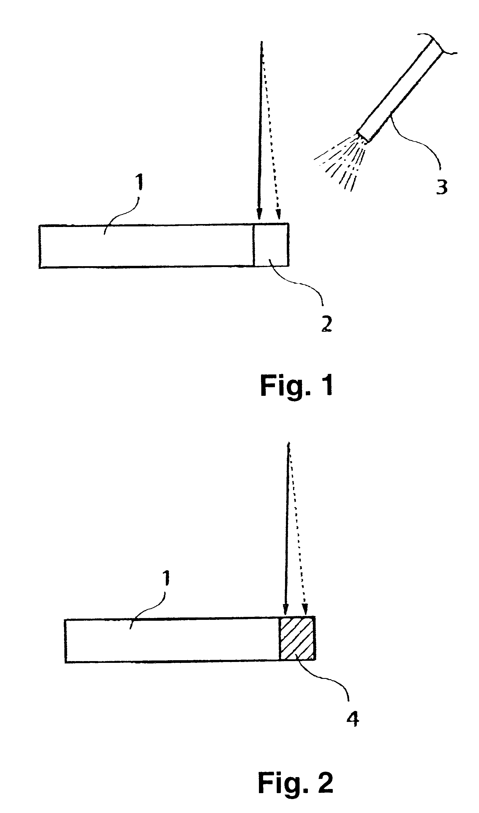
(4) For repair of clear defects, suitable materials, which scatter electrons as the membrane does and does not absorb electrons, should be supplied to the defects. So far such suitable materials with proper structure and the method for providing such materials are not selected or established.
In this case, the
corrosion might prevail upon a part other than a beam
irradiation zone, and a desirable processing shape cannot be obtained when the gas-assist
etching is performed on the opaque defect by irradiating the
focused ion beam to the opaque defect.
As a result, a processing resolution in the order of submicron cannot be effectively achieved.
However, since
iodine is very corrosive to a
boron-doped-
silicon, the amount of gas supplied to the vicinity of a portion to be processed needs to be fine-tuned.
It is, however, unavoidable that the membrane density of an obtainable membrane forming material is lower compared with the density of bulk (reticle material) even if the
focused ion beam, the electron beam, or the infinitesimal
plasma is used as an
exposure source.
For membrane formed in this condition, it is unavoidable that the
electron scattering property becomes lower than the
electron scattering property of bulk if the membrane density is low, even though the membrane is composed only of
silicon, carbon, or a mixture thereof without containing impurities.
This kind of membrane is not sufficient as an electron beam scatterer material.
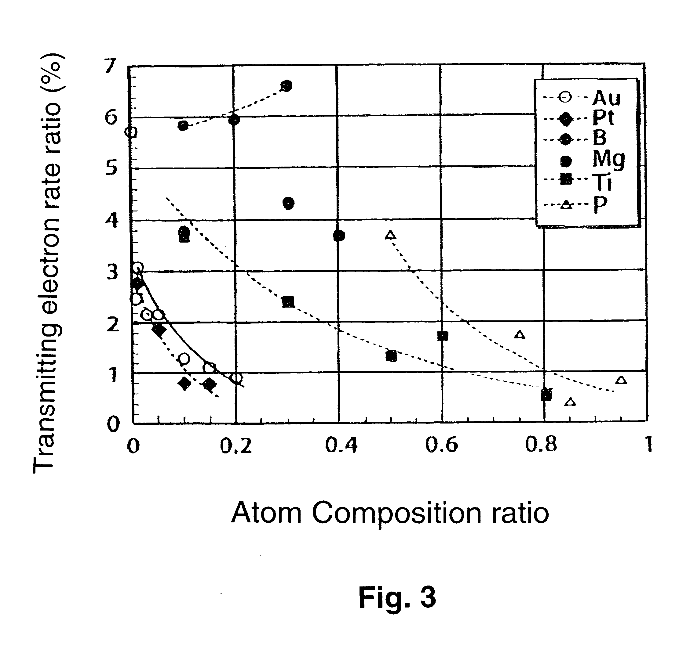
However, careful attention should be paid not to add an excessive amount of elements because as the absorption quantity of electrons increases, it may result in generation of heat.
On the other hand, the electron scattering property of these elements also increases when excessive elements are added.

