Plane switching liquid crystal displaying apparatus for improved luminance

a liquid crystal display and plane switching technology, applied in static indicating devices, instruments, non-linear optics, etc., can solve the problems of changing the vertical luminance of the window portion, the picture quality is worse, and the array substrate is inferior, so as to improve the shielding effect, and reduce the light shielding area.

Inactive Publication Date: 2002-09-17
MITSUBISHI ELECTRIC CORP
View PDF12 Cites 77 Cited by
  • Summary
  • Abstract
  • Description
  • Claims
  • Application Information

AI Technical Summary

Benefits of technology

The first object of the present invention is to solve the problems mentioned above, and to provide an IPS liquid crystal displaying apparatus causing electric field parallel to a glass substrate, the IPS liquid crystal displaying apparatus capable of improving shielding effect against electric field leaking from the signal line, making the

Problems solved by technology

The electric field is caused along the surface of the glass substrate 1, thus causing a problem like crosstalk.
For example, when a white window is displayed in such black displaying as shown in FIG. 47, there prises a problem on the display called "longitudinal crosstalk" where the vertical luminance of the window portion changes with respect to the other black displaying portion.
Thus, uneven luminance is likely to be caused, causing the picture quality to worsen.
The level difference provided makes not only the array substrate inferior due to cracking, but also disconnects the wiring on the array substrate due to the level difference portion in the manufacturing operation with a problem in im

Method used


Image

  • Plane switching liquid crystal displaying apparatus for improved luminance
  • Plane switching liquid crystal displaying apparatus for improved luminance
  • Plane switching liquid crystal displaying apparatus for improved luminance

Examples


embodiment 1

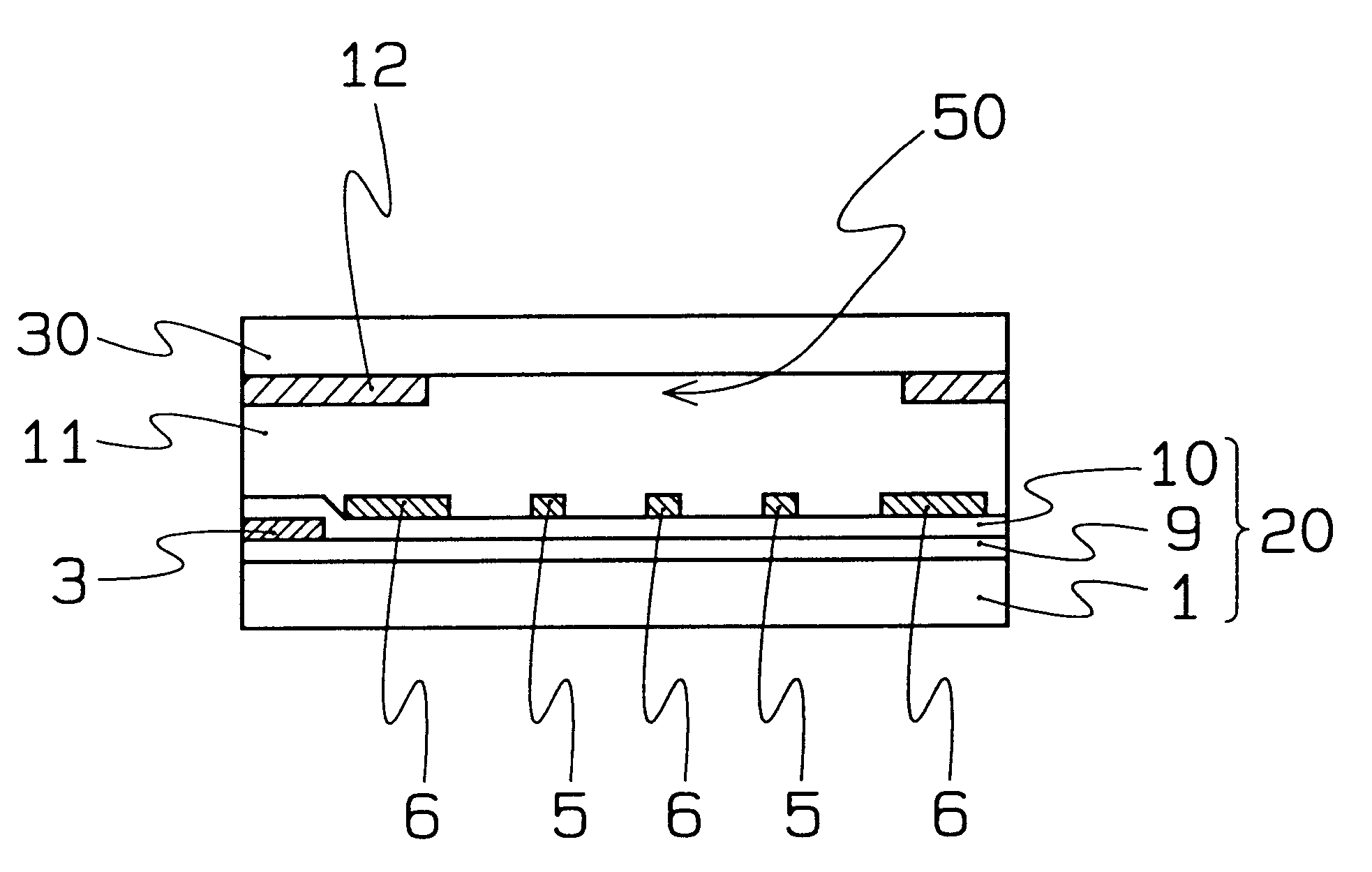
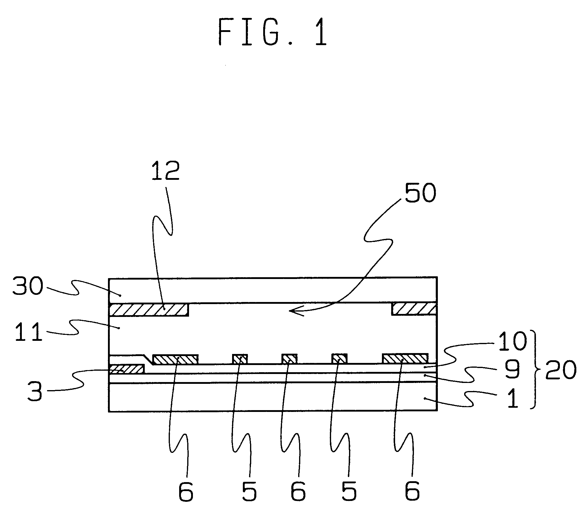
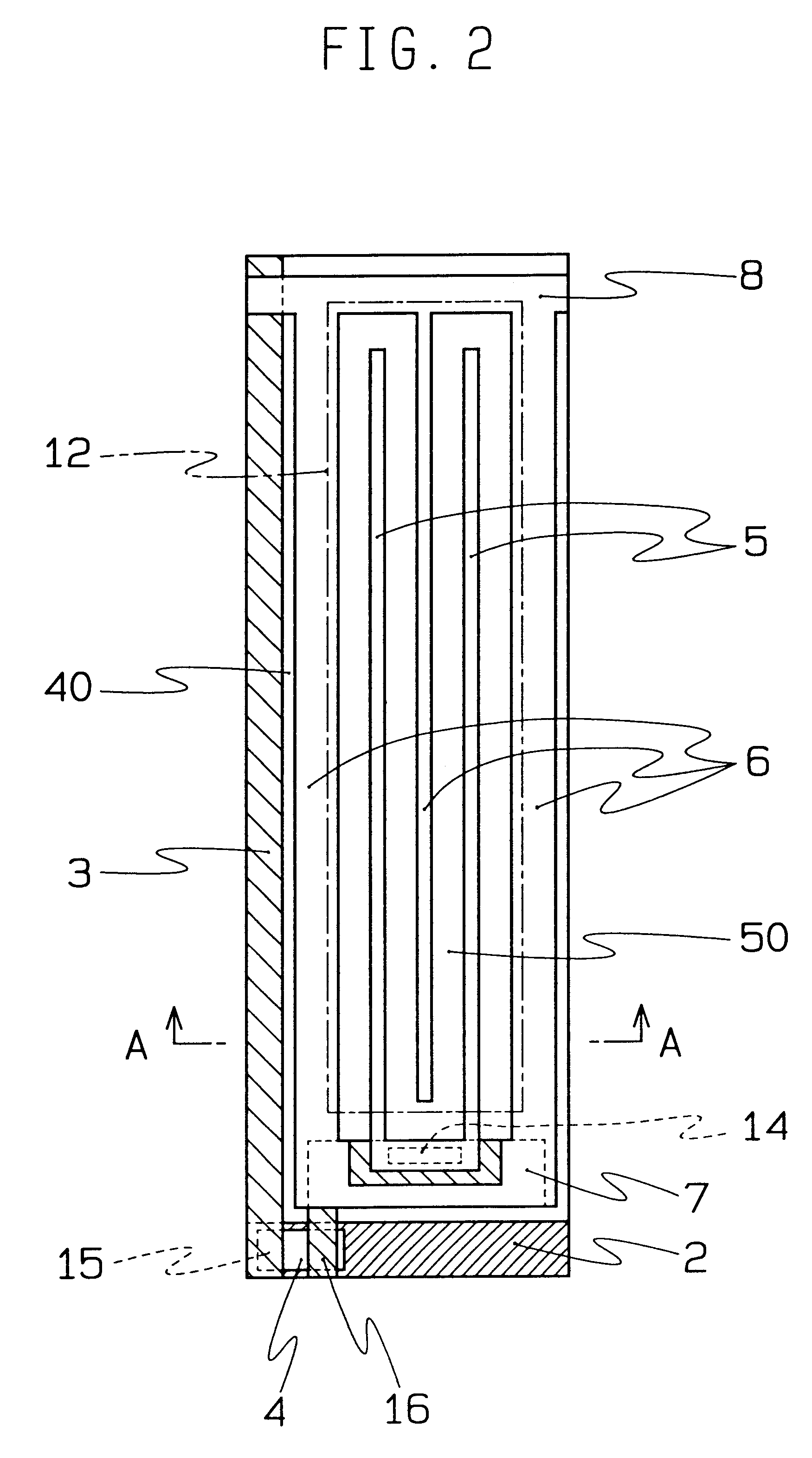
One embodiment of the present invention will be described in accordance with drawings. The reference numerals in Embodiment 1 are the same as those of the conventional reference numerals. FIG. 1 is a sectional view showing the construction of one pixel of the IPS type liquid crystal displaying apparatus in Embodiment 1 of the present invention. FIG. 2 is its plain view. FIG. 1 is a sectional view taken along a line of A--A in FIG. 2. Referring to the drawing, reference numeral 1 denotes a glass substrate, numeral 2 denotes a scanning line, numeral 3 denotes a signal line, numeral 4 denotes a TFT, numeral 5 denotes a driving electrode, numeral 6 denotes an opposite electrode, numeral 7 denotes an electrode for forming the storage capacitance, numeral 8 denotes a common line, numeral 9 denotes a gate insulating film, numeral 10 denotes a passivation film, numeral 11 denotes a liquid crystal, numeral 12 denotes a block matrix BM, numeral 14 denotes a contact hole, numeral 15 denotes a ...

embodiment 2

FIGS. 19a and 19b show the construction of the pixel electrode of the liquid crystal displaying apparatus of the embodiment 2 of the present invention. FIG. 19a is its plain view. FIG. 19b is a sectional view taken along a line of A--A of FIG. 19a. FIGS. 20a, 20b, 21a, 21b, 22a, 22b, 23a, 23b, 24a and 24b are views showing the process flow of the array substrate. Referring to the drawing, reference numeral 1 denotes a glass substrate, numeral 2 denotes a scanning line, numeral 3 denotes a signal line, numeral 4b denotes a channel region, numeral 5 denotes a driving electrode, numeral 6 denotes an opposite electrode, numeral 7 denotes an electrode for forming the storage capacitance, numeral 8 denotes a common line, numeral 9 denotes a gate insulating film, numeral 10 denotes a passivation film, numeral 11 denotes a liquid crystal, numeral 12 denotes a BM, numeral 14 denotes a contact hole, numeral 15 denotes a source electrode of a transistor, and numeral 16 denotes a drain electrod...

embodiment 3

FIGS. 25a and 25b show the construction of one pixel of the liquid crystal displaying apparatus of the embodiment 2 of the present invention. FIG. 25a is its plain view. FIG. 25b is a sectional view taken along a line of A--A of FIG. 25a. FIGS. 26a, 26b, 27a, 27b, 28a, 28b, 29a, 29b, 30a and 30b are views showing the process flow of the array substrate. Referring to the drawing, reference numeral 1 denotes a glass substrate, numeral 2 denotes a scanning line, numeral 3 denotes a signal line, numeral 4b denotes a channel region, numeral 5 denotes a driving electrode, numeral 6 denotes an opposite electrode, numeral 7 denotes an electrode for forming the storage capacitance, numeral 8 denotes a common line, numeral 9 denotes a gate insulating film, numeral 10 denotes a passivation film, numeral 11 denotes a liquid crystal, numeral 12 denotes a BM, numeral 14 denotes a contact hole, numeral 15 denotes a source electrode of a transistor, and numeral 16 denotes a drain electrode. Numeral...


PUM


Abstract

An IPS liquid crystal displaying apparatus includes: a TFT array substrate, an opposite substrate opposed to the TFT array substrate and liquid crystal interposed between the TFT array substrate and the opposite substrate, wherein the TFT array substrate is composed of a glass substrate, a gate insulating film formed on the glass substrate, a possivation film formed on the gate insulating film, a plurality of scanning lines for transmitting a scanning signal, a plurality of signal lines for transmitting an image signal, a plurality of pixels arranged in grid like pattern by crossing the plurality of scanning lines with the plurality of signal lines, a plurality of TFTs implementing switching operation of the image signal on the basis of the scanning signals, a plurality of driving electrodes connected with the TFT, a plurality of opposite electrodes arranged in such a manner that each of the plurality of opposite electrodes is opposed to each of the driving electrodes, and a plurality of common lines for mutually connecting each of the opposite electrode of one of the plurality of pixels with the other one of the plurality of pixels, wherein the TFT array substrate is formed on the passivation film, the passivation film being different from a layer provided with the driving electrode and the opposite electrode.

Description

BACKGROUND OF THE INVENTIONField of the InventionThe present invention relates to an IPS (In Plane Switching) liquid crystal displaying apparatus by generating an electric field parallel to an array substrate to drive the liquid crystal. More particularly, the present invention relates to a construction of a highly bright liquid crystal displaying apparatus increased in aperture ratio by reducing influences of the leakage of electric field from a signal line, thereby reducing the light shielding area.DISCUSSION OF BACKGROUNDIn an active matrix type liquid crystal displaying apparatus, an IPS system where the direction of the electric field to be applied on the liquid crystal is made parallel to the array substrate is mainly used as a method of obtaining a wider viewing angle (for example, see Japanese Unexamined Patent Publication No. 254712 / 1996). It is reported that this system removes almost all of the change in the contrast and the inversion of the gradation level in changing th...

Claims


Application Information

Patent Timeline
IPC IPC(8): G02F1/1343G02F1/13G02F1/1362G02F1/136G02F1/1368
CPCG02F1/134363G02F1/136227G02F1/136286
Inventor NIWANO, YASUNORIMASUTANI, YUICHINAKASHIMA, KENOODOI, YUUZOUKOBAYASHI, KAZUHIRO
Owner MITSUBISHI ELECTRIC CORP
Why Eureka
Try Eureka