Antifuse for use with low k dielectric foam insulators

a foam insulator and dielectric foam technology, applied in the field of fuse elements, can solve the problems of high electrical resistance, void compression, and interruption of line continuity

Inactive Publication Date: 2002-10-01
GLOBALFOUNDRIES INC
View PDF21 Cites 34 Cited by
  • Summary
  • Abstract
  • Description
  • Claims
  • Application Information

AI Technical Summary

Problems solved by technology

The molten metal then boils, vaporizes or explodes out of its oxide surroundings, disrupting line continuity and causing high electrical resistance.
Any porous materials in contact with the fuse link will experience compression of the voids with subsequent loss of pressure.
However, low k dielectrics will collapse catastrophically at the energy levels required to laser current blow fuses leading to various reliability if not yield d...

Method used


Image

  • Antifuse for use with low k dielectric foam insulators
  • Antifuse for use with low k dielectric foam insulators
  • Antifuse for use with low k dielectric foam insulators

Examples


Embodiment Construction

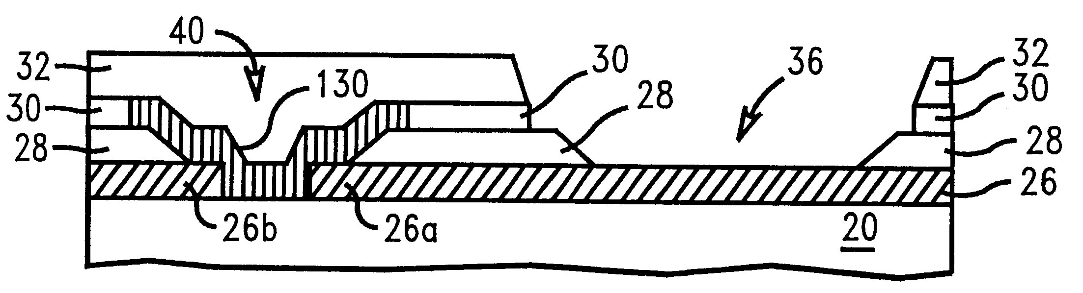
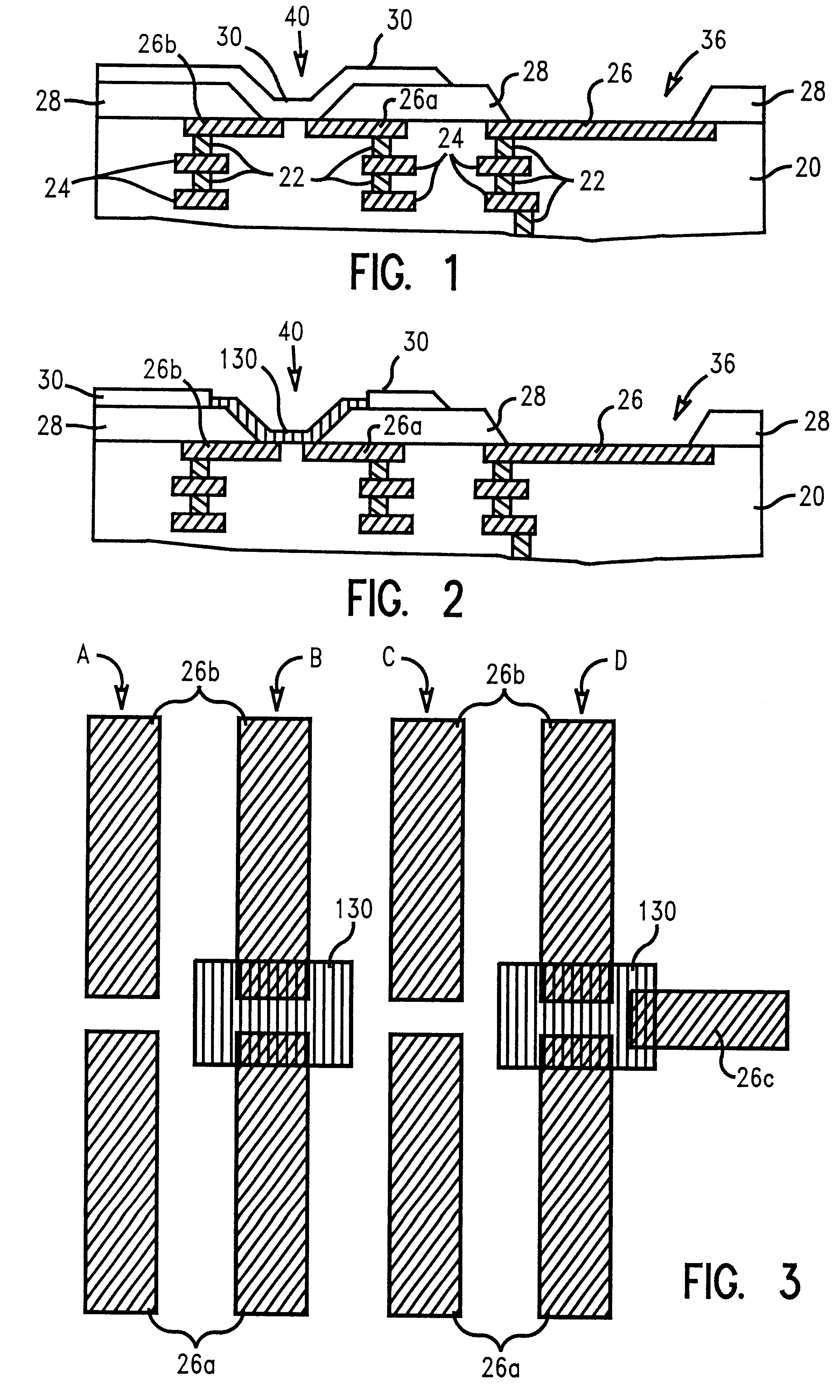
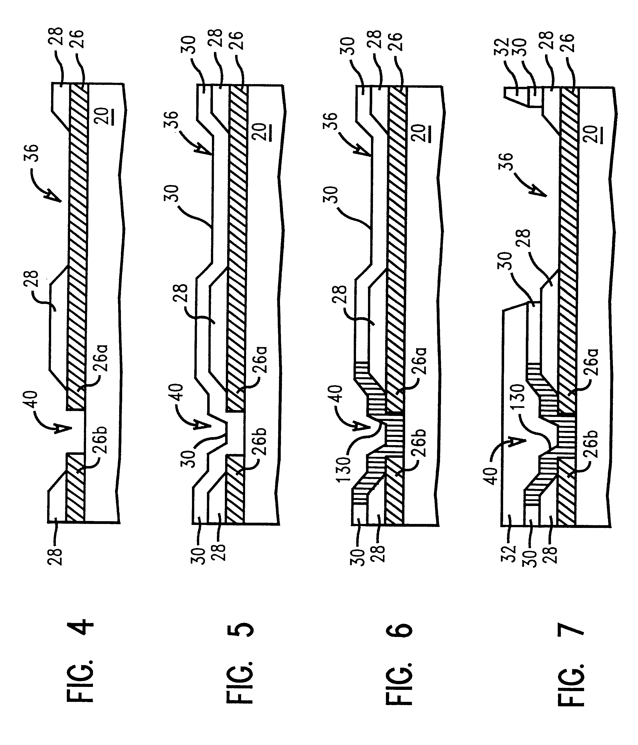
An example of how the fuse structure of the present invention may be formed is provided below.

Initially, a nanopore glass is deposited as the underlayer dielectric. If desired, a thin layer of full density silicon dioxide, silicon nitride, or the like can be deposited as a cap over the nanopore glass layer. Using conventional resist techniques, trenches are etched in the glass to define the wiring pattern, and the resist is then stripped. Using a damascene process, the trenches are filled with one or more metals, e.g. copper, to define the conduction wires. Using chemical mechanical polishing, the unwanted metal is removed from the field areas. A nanopore glass is then deposited as the overcoat dielectric. If desired, a thin layer of full denisity silicon dioxide., silicon nitride, or the like can be deposited as a barrier under the nanopore glass, and a second thin layer of full density silicon dioxide, silicon nitride, or the like can be deposited as a cap over the nanopore glass....


PUM


Abstract

A fusible link for a semiconductor device comprises an insulating substrate and a conductive line pair on the surface of the insulating substrate, with the conductive line pair having spaced ends. A polymer is disposed over the insulating substrate and between the conductive line pair ends. The polymer is capable of being changed from a non-conductive to a conductive state upon exposure to an energy beam. Preferably, the polymer comprises a polyimide, more preferably, a polymer/onium salt mixture, most preferably, a polyaniline polymer doped with a triphenylsufonium salt. The link may further comprise a low k nanopore/nanofoam dielectric material adjacent the conductive line ends.

Description

1. Field of the InventionThis invention relates to a fuse element used in integrated circuit (IC) devices and, more particularly, to a fuse structure and method of making the fuse which employs a local change in electrical conductivity of a film in contact with metal lines.2. Description of Related ArtFuses are used in integrated circuit devices such as semiconductor chips to provide redundancy, electrical chip identification and customization of function. For designs having three or more layers of wiring, the fuses are typically formed from a segment of one of the wiring layers, e.g., the "last metal" or "last metal minus one" wiring layer. Fusing, i.e., deletion of a segment of metal fuse line, is accomplished by exposing the segment to a short, high intensity pulse of "light" from an infra-red laser. The molten metal then boils, vaporizes or explodes out of its oxide surroundings, disrupting line continuity and causing high electrical resistance. A sensing circuit is used to dete...

Claims


Application Information

Patent Timeline
IPC IPC(8): H01L23/532H01L23/525H01L23/52
CPCH01L23/5254H01L23/5329H01L2924/0002H01L2924/00
Inventor DAUBENSPECK, TIMOTHY H.KLAASEN, WILLIAM A.MOTSIFF, WILLIAM T.PREVITI-KELLY, ROSEMARY A.RANKIN, JED H.
Owner GLOBALFOUNDRIES INC
Why Eureka
Try Eureka