
Contact array structure for buried type transistor

Inactive Publication Date: 2002-10-01
MACRONIX INT CO LTD
View PDF11 Cites 34 Cited by
  • Summary
  • Abstract
  • Description
  • Claims
  • Application Information

AI Technical Summary

Benefits of technology

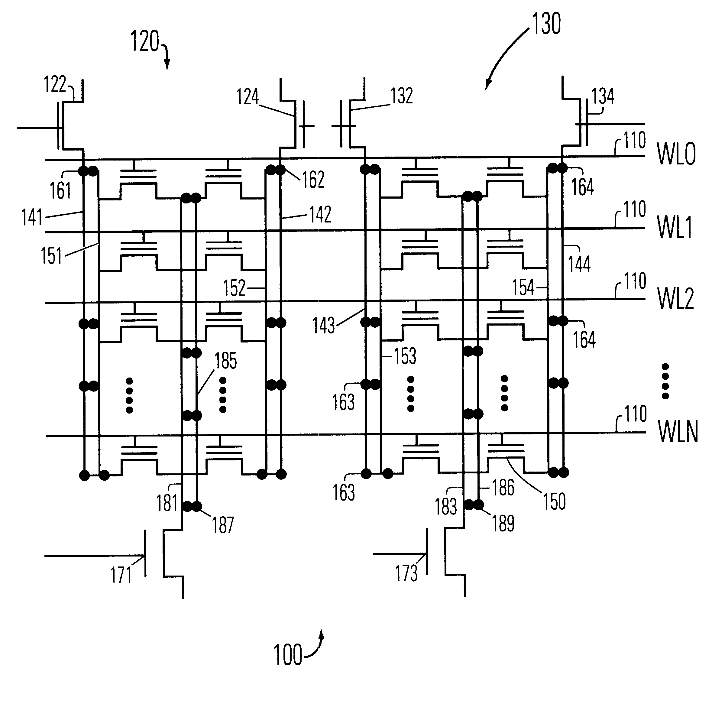
A buried transistor array with a contact structure, representing an embodiment of the invention, can be cost effective and advantageous for at least the following reasons. The invention reduces buried diffusion line resistance, particularly in high current applications such as writing with hot electron (hot e) programming on an EPROM or FLASH EPROM. The invention enhances read current and read speed when longer buried diffusion lines are used. This enhancement of read current and speed is particularly beneficial for buried types, such as, for example, MROM, EPROM, FLASH EPROM and FLASH EEPROM types. The invention tightens the voltage-time (VT) distribution, particularly when writing with hot electron programming on an EPROM or FLASH EPROM by putting a contact in communication with the buried diffusion bit line to reduce the drain voltage distinction between the first buried transistor cell and the last buried transistor along a given buried drain diffusion bit line.All publications, patent applications, and issued patents mentioned in this application are hereby incorporated herein by reference in their entirety to the same extent as if each individual publication, application, or patent was specifically and individually indicated to be incorporated in its entirety by reference.All the disclosed embodiments of the invention described herein can be realized and practiced without undue experimentation. Although the best mode of carrying out the invention contemplated by the inventors is disclosed above, practice of the present invention is not limited thereto. Accordingly, it will be appreciated by those skilled in the art that the invention may be practiced otherwise than as specifically described herein.For example, the individual components need not be formed in the disclosed shapes, or assembled in the disclosed configuration, but could be provided in virtually any shape, and assembled in virtually any configuration. Further, the individual components need not be fabricated from the disclosed materials, but could be fabricated from virtually any suitable materials. Further, although the contact array structure described herein is a physically separate module, it will be manifest that the contact array may be integrated into the circuitry with which it is associated. Furthermore, all the disclosed elements and features of each disclosed embodiment can be combined with, or substituted for, the disclosed elements and features of every other disclosed embodiment except where such elements or features are mutually exclusive.It will be manifest that various additions, modifications and rearrangements of the features of the present invention may be made without deviating from the spirit and scope of the underlying inventive concept. It is intended that the scope of the invention as defined by the appended claims and their equivalents cover all such additions, modifications, and rearrangements. The appended claims are not to be interpreted as including means-plus-function limitations, unless such a limitation is explicitly recited in a given claim using the phrase "means-for." Expedient embodiments of the invention are differentiated by the appended subclaims.

Problems solved by technology

A previously recognized problem with this diffusion bit line technology has been there can be significant voltage drops along such bit lines.
Specifically, the voltage drop is severe for high current applications such as, for example, writing with hot electron programming on EPROM or FLASH EPROM circuits.
Another previously recognized problem with this diffusion bit line technology has been that the read current and the read speed of circuits with longer buried diffusion lines are too low.
Another previously recognized problem with this diffusion bit line technology has been that the voltage / time (VT) distribution when writing to transistors connected with such buried diffusion lines by means of hot electron programming is unsatisfactorily wide.
Heretofore, the above-discussed requirements of reduced resistance, improved read current and speed, and tightened VT distribution have not been fully met.

Method used


Image

  • Contact array structure for buried type transistor
  • Contact array structure for buried type transistor
  • Contact array structure for buried type transistor

Examples


Embodiment Construction

The present invention and the various features and advantageous details thereof are explained more fully with reference to the nonlimiting embodiments that are illustrated in the accompanying drawings and detailed in the following description. Descriptions of well known components and processing techniques are omitted so as not to unnecessarily obscure the present invention in detail.

A detailed description of a preferred embodiment of the invention is provided with respect to FIGS. 1 and 5-9. In general, the invention is directed to incorporating embedded contacts and conductors associated therewith into electrical contact with one, or more, buried diffusion bit lines. The contacts are structures that function as electronic conduits. The contacts and the associated conductors are configured to provide at least one route of lower resistance compared to the situation where only the buried diffusion bit lines are present.

Referring now to FIG. 1, a schematic circuit diagram representing...


PUM


Abstract

Systems and methods are described for providing an array of buried transistor cells with at least one contact array structure. A contact array structure for a buried type transistor array includes a first diffusion bit line coupled to the plurality of transistors; a first plurality of contacts coupled to the source diffusion bit line; and a first conductor coupled to the first plurality of contacts. The systems and methods provide advantages in that the diffusion line resistance is reduced, the read current and speed are reduced, and the voltage-time distribution is tightened when writing by hot electron programming.

Description

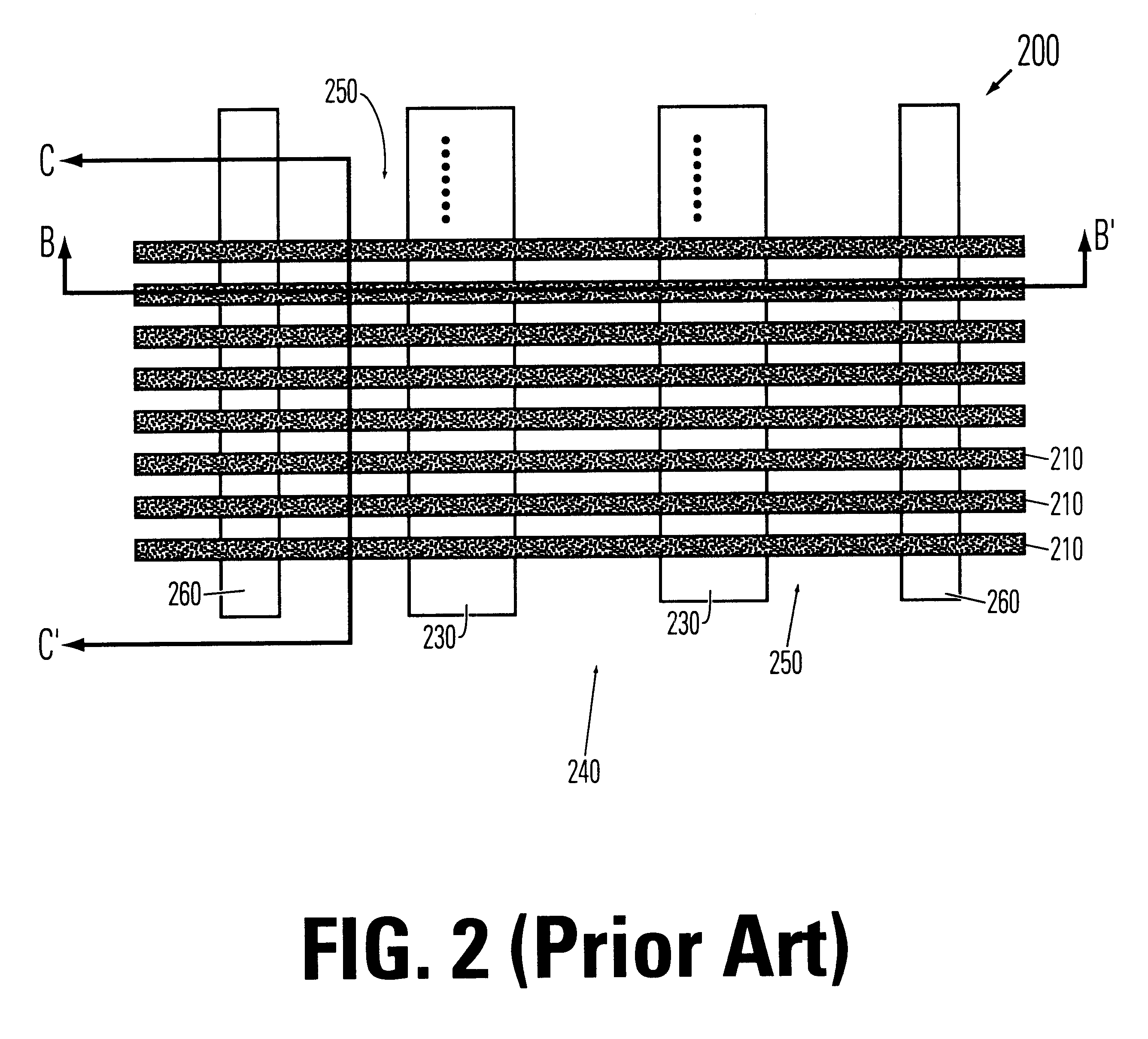
1. Field of the InventionThe present invention relates generally to the field of buried transistor circuits. More particularly, the present invention relates to an array of buried transistor cells including diffusion bit lines that are provided with a contact array structure for reducing resistance along the diffusion bit lines. Specifically, a preferred implementation of the present invention relates to floating gate (e.g., FLASH EPROM) memories that include a contact array structure that parallels one, or more, diffusion bit lines.2. Discussion of the Related ArtIt has been known in the field of microelectronics to connect buried transistors with diffusion bit lines. Prior art diffusion bit lines, sometimes called bit lines, are well known to those skilled in the art. U.S. Pat. Nos. 4,597,060; 5,399,891; 5,453,391; and 5,526,307, disclose floating gate memory circuits composed of buried transistor cells connected together with diffusion bit lines.For instance, referring to FIG. 2,...

Claims


Application Information

Patent Timeline
IPC IPC(8): G11C7/00G11C7/18H01L27/115
CPCG11C7/18H01L27/115H10B69/00
Inventor HUANG, CHIN-YICHANG, YUN
Owner MACRONIX INT CO LTD
Learn More