Oxynitride laminate "blocking layer" for thin film semiconductor devices

a technology of oxynitride and semiconductor devices, which is applied in the direction of semiconductor devices, electrical devices, transistors, etc., can solve the problems of low power consumption, operation fault, and charge loss

Inactive Publication Date: 2002-10-08
SEMICON ENERGY LAB CO LTD
View PDF25 Cites 187 Cited by
  • Summary
  • Abstract
  • Description
  • Claims
  • Application Information

AI Technical Summary

Problems solved by technology

The smaller the S value is, the faster it is possible to operate the TFT, and the lower its power consumption becomes.
Furthermore, in a shift register circuit formed in a driver circuit, if the S value is large (if the sub-threshold characteristics are poor), then charge loss occurs due to the leak current, and this causes a fatal operation fault.
The circuit becomes impossible to operate.
If the quality of the blocking layer is poor, the ions then easily mix into the active layer, change the electrical characteristics of the TFT, and the reliability cannot be maintained over time.
If a silicon nitride film is used as the blocking layer, then the blocking effect of impurity ions is high, but there are many trap levels, and further, the internal stress is large.
Therefore, there is a fear of problems developing with the TFT characteristics if a silicon nitride film is formed directly contacting the active layer.
However, a silicon oxide film has disadvantages of moisture absorbency, and a low blocking effect against impurity ions.
As a result, it becomes impossible to operate the TFT at the desired voltage.
A channel dope is a method which is effective in controlling V.sub.th, but if V.sub.th shifts to the order of -4 to -3 V when a circuit such as a CMOS circuit is formed by forming both an n-channel TFT and a P-channel TFT on the same substrate, then it is difficult to control the V.sub.th of both TFTs with one channel dope.
If channel doping is performed twice, the number of process steps increases, and this is a cause of increases manufacturing costs.
However, if the ratio of nitrogen contained in the silicon oxynitride film is raised, then the trap levels are increased, and further, the internal stress becomes large, so that it is not suitable to form the active layer directly contacting this film.

Method used


Image

  • Oxynitride laminate "blocking layer" for thin film semiconductor devices
  • Oxynitride laminate "blocking layer" for thin film semiconductor devices
  • Oxynitride laminate "blocking layer" for thin film semiconductor devices

Examples


embodiment 1

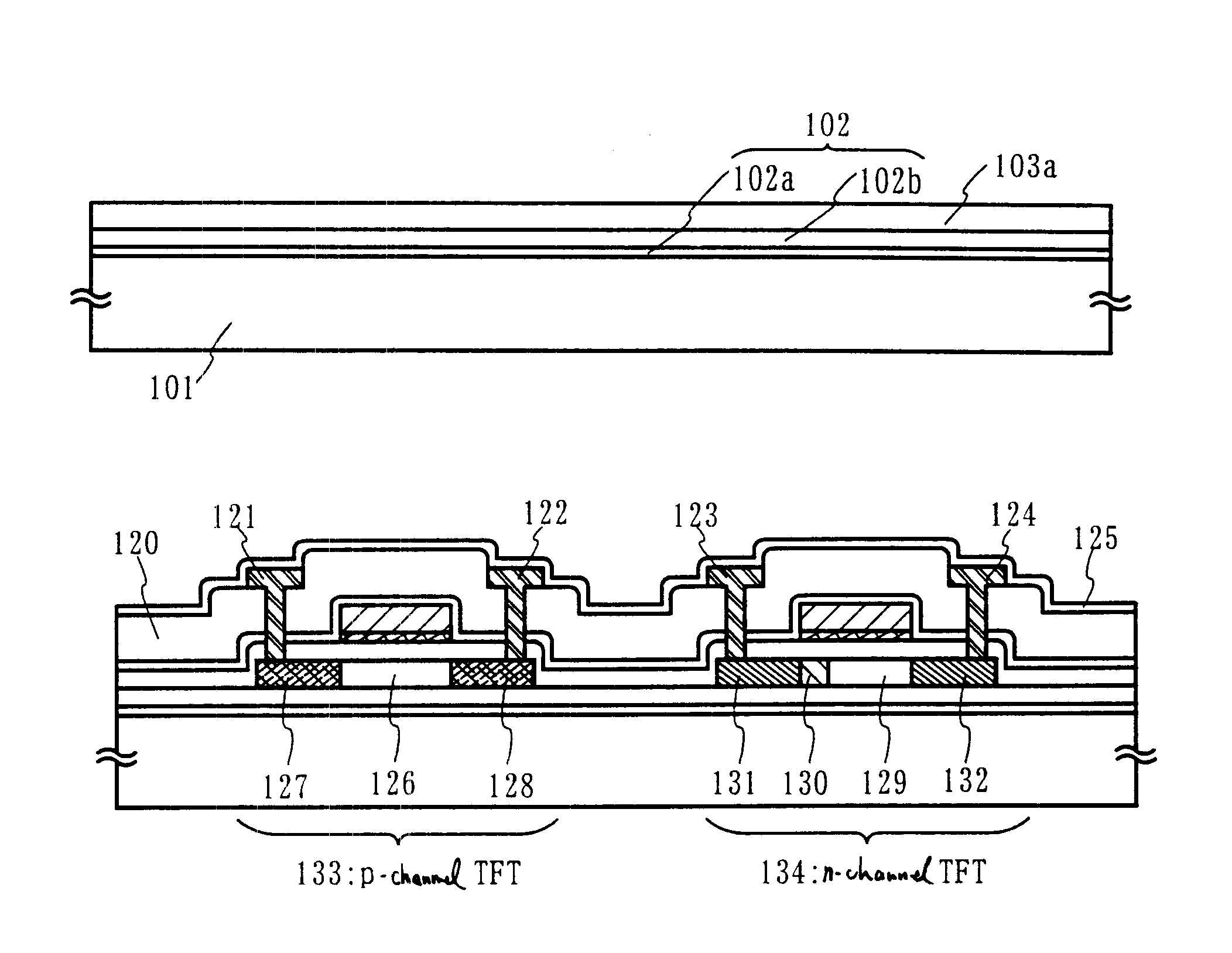
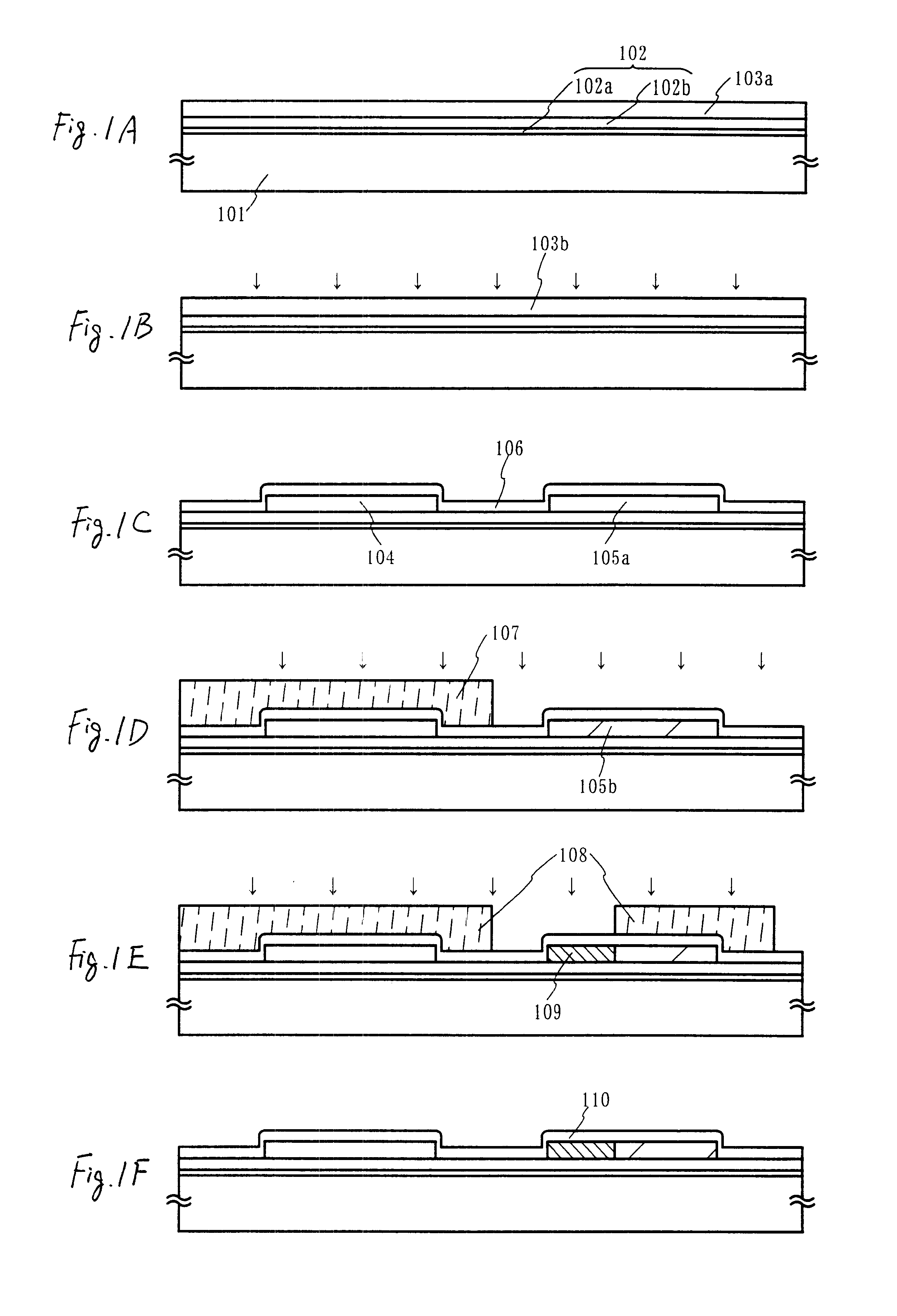
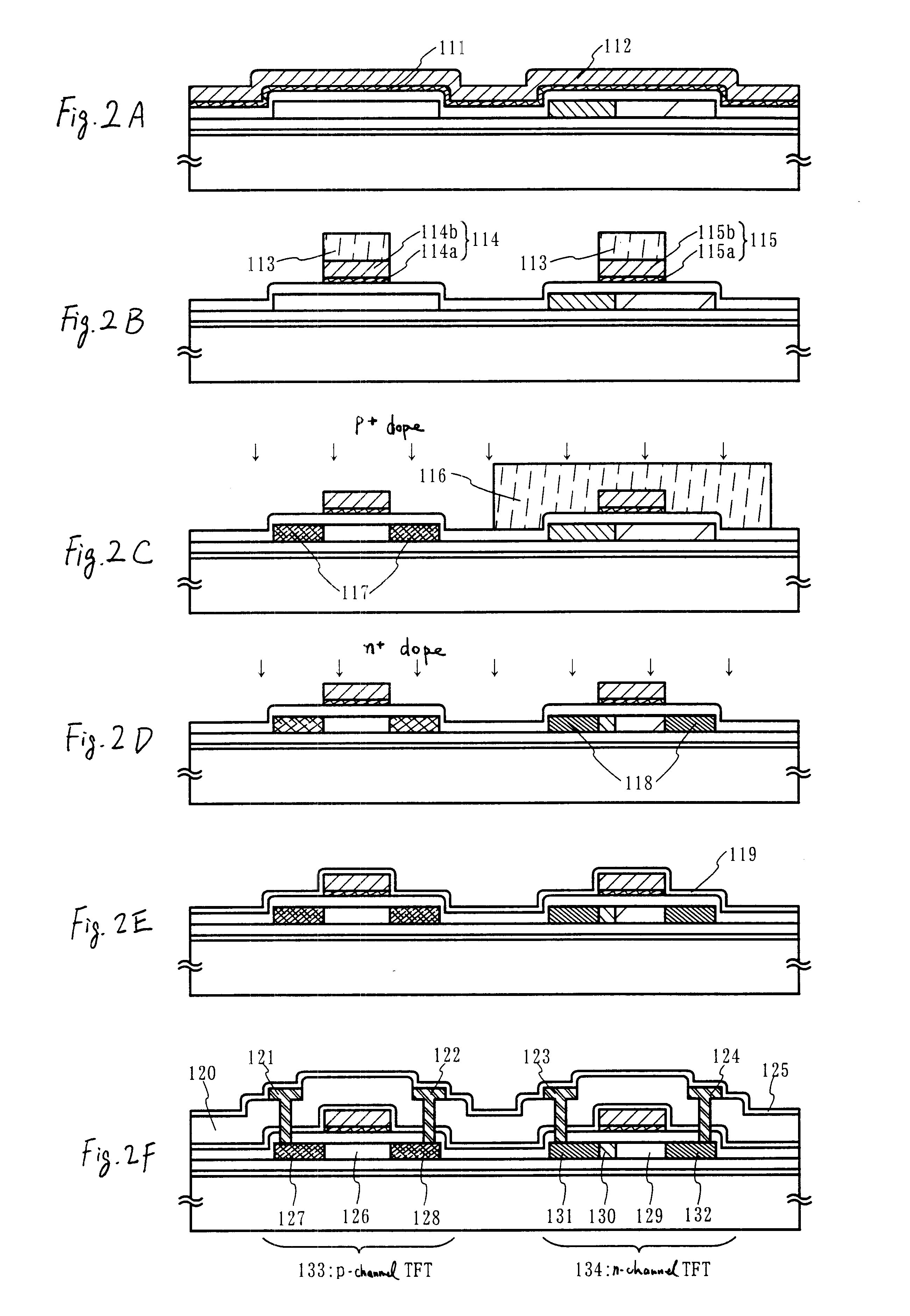
Embodiment 1 of the present invention is explained using FIGS. 8A to 12. Here, a detailed explanation is made of a method of manufacturing a pixel TFT of a pixel portion, and driver circuit TFTs formed in the periphery of the pixel portion. Note that, in order to simplify the explanation, a CMOS circuit, which is the basic circuit for control circuits such as a shift register circuit and a buffer circuit, and an n-channel TFT forming a sampling circuit are shown in the figures.

A barium borosilicate glass substrate or an aluminum borosilicate glass substrate is used as a substrate 201 in FIG. 8A. An aluminum borosilicate glass substrate is used in embodiment 1. Heat treatment may be performed in advance at a temperature which is lower than the distortion point of the glass by 10 to 20.degree. C. A blocking layer 202 is formed on the substrate 201 by forming a silicon oxynitride film (A) 202a with a thickness of 50 nm on the surface of the substrate 201 on which the TFTs are formed, a...

embodiment 2

In embodiment 2, a process of manufacturing an active matrix liquid crystal display device from the active matrix substrate of embodiment 1 is explained. As shown in FIG. 18, an alignment film 601 is formed for the active matrix substrate in the state of FIG. 12. A polyimide resin is often used for the alignment film of a liquid crystal display device. A light shielding film 603, a transparent conducting film 604, and an alignment film 605 are formed on an opposing substrate 602. After forming the alignment films, a rubbing process is performed to give the liquid crystal molecules a certain fixed pre-tilt angle, bringing them into alignment. The active matrix substrate, on which the pixel matrix circuit and the CMOS circuit are formed, and the opposing substrate are then joined together by a sealing material or spacers (both not shown in the figures)in accordance with a known cell construction process. Next, a liquid crystal material 606 is injected between both substrates, and the ...

embodiment 3

FIG. 17 is a view showing an example of the arrangement of input-output terminals, a display region, and driver circuits of a liquid crystal display device. There are m gate wirings and n source wirings that intersect in a matrix shape in the pixel portion 406. For example, 480 gate wirings and 640 source wirings are formed when the pixel density is VGA, and 768 gate wirings and 1024 source wirings are formed for the case of XGA. The screen size of the display region becomes 340 mm for a 13-inch class in diagonal length, and becomes 460 mm for an 18-inch class in diagonal. It is necessary to form the gate wirings from low resistance materials as shown in embodiment 1 in order to realize this kind of liquid crystal display device. If the time constant (resistance.times.capacitance) of the gate wirings becomes large, then the response speed of the scanning signal becomes slow, and the liquid crystal cannot be driven at high speed. For example, when the material forming the gate wiring...


PUM


Abstract

Channel doping is an effective method for controlling Vth, but if Vth shifts to the order of -4 to -3 V when forming circuits such as a CMOS circuit formed from both an n-channel TFT and a P-channel TFT on the same substrate, then it is difficult to control the Vth of both TFTs with one channel dope. In order to solve the above problem, the present invention forms a blocking layer on the back channel side, which is a laminate of a silicon oxynitride film (A) manufactured from SiH4, NH3, and N2O, and a silicon oxynitride film (B)manufactured from SiH4and N2O. By making this silicon oxynitride film laminate structure, contamination by alkaline metallic elements from the substrate can be prevented, and influence by stresses, caused by internal stress, imparted to the TFT can be relieved.

Description

1. Field of the InventionThe present invention relates to a semiconductor device formed by a circuit made from a thin film transistor (hereafter referred to as TFT) formed on a substrate, and a method of manufacturing thereof. In particular, the present invention relates to an insulating film formed between a semiconductor layer which is an active layer of the TFT, and the substrate. This kind of insulting film is referred to as a blocking layer or a base film. Along with obtaining good TFT characteristics, the present invention relates to a suitable insulating film structure for preventing deterioration of the TFT, and the method of its manufacture.The semiconductor device of the present invention includes a display device having a TFT or a semiconductor circuit including TFTs, and an electro-optical device such as an image sensor. In addition, the semiconductor device of the present invention also includes electronic equipment loaded with these display devices and electro-optical ...

Claims


Application Information

Patent Timeline
Patent Type & Authority Patents(United States)
IPC IPC(8): H01L21/70H01L27/12H01L21/84H01L21/77H01L29/04H01L29/786
CPCH01L27/12H01L29/78603H01L29/78621H01L29/78624H01L29/78627H01L27/1248
Inventor KITAKADO, HIDEHITOHAYAKAWA, MASAHIKOYAMAZAKI, SHUNPEIASAMI, TAKETOMI
Owner SEMICON ENERGY LAB CO LTD
Why Eureka
Try Eureka