Semiconductor device capable of generating highly precise internal clock

a technology of internal clock and semiconductor device, which is applied in the direction of generating/distributing signals, digital storage, instruments, etc., can solve the problems of unable to meet the operating speed of microprocessors (mpus), the inability to provide a more rapid internal clock signal for use internal to an sdram, and the inability to meet the requirements of microprocessors (mpus)

Inactive Publication Date: 2002-12-03
MITSUBISHI ELECTRIC CORP
View PDF5 Cites 105 Cited by
  • Summary
  • Abstract
  • Description
  • Claims
  • Application Information

AI Technical Summary

Problems solved by technology

However, its operating speed still cannot catch up to that of microprocessors (MPUs).
Thus it is often said that the DRAM's access time and cycle time become a bottleneck and the entire system is degraded in performance.
As an MPU operates more and more rapidly, as has been described above, providing a more rapid internal clock signal for use internal to an SDRAM is an unavoidable issue in terms of the performance of the entire system as well as other aspects, since if an internal clock signal is slow an access time from a clock governs an operating frequency.
A DLL of digital type is considered suitable since in an SDRAM, which would suffer large power-supply noise, a DLL of analog type would result in large jitter or fluctuation attributed to the noise.
For a high operating frequency, a conventional delay line, having a delay time varying in too large a step, can disadvantageously provide the delay time varying stepwise, resulting in no operating margin.
Furthermore, for a high operating frequency, locking a DLL requires a delay time shorter than the minimal delay.
As such, the internal clock signal is limited in having high rate.

Method used


Image

  • Semiconductor device capable of generating highly precise internal clock
  • Semiconductor device capable of generating highly precise internal clock
  • Semiconductor device capable of generating highly precise internal clock

Examples


first embodiment

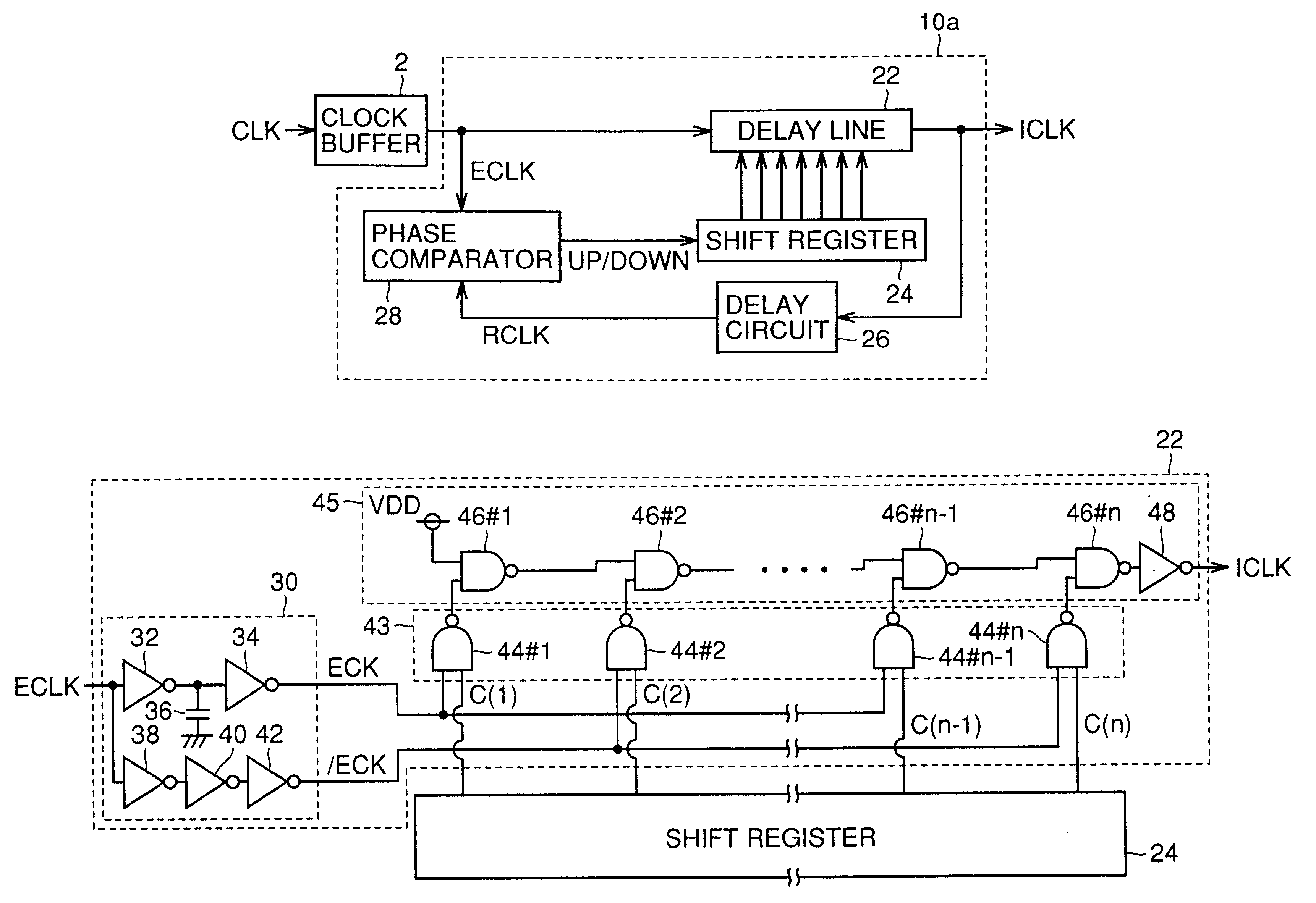
FIG. 1 is a block diagram showing a schematic configuration of a semiconductor device 1 in the present invention.

As shown in FIG. 1, semiconductor device 1 is shown as exemplary, synchronous dynamic random access memory (SDRAM) synchronized with a clock signal to communicate data. Semiconductor 1 includes a clock buffer 2 receiving an external clock signal CLK and a clock enable signal CKE, an address buffer 4 receiving address signals A0-An (n is a natural number) and bank address signals BA0-BAn, and a control signal buffer 6 receiving control signals / CS, / RAS, / CAS, / WE, DQM. Address buffer 4 and the control buffer are synchronized with an output of clock buffer 2 to take in an address signal, a control signal and the like.

Semiconductor device 1 also includes an internal clock generation circuit 10 generating an internal clock signal in response to an output of clock buffer 2, a control circuit 8 synchronized with an output of clock buffer 2 to receive an output of address buffe...

second embodiment

When the power is turned on, with the delay line having its amount of delay set to be minimal, the DLL circuit starts adjusting a delay time, since locking with a large amount of delay would increase jitter. The delay line has an amount of delay varying depending on noise introduced into power supply potential. If the delay line provides a larger amount of delay, depending on the noise the amount of delay has a larger variation. As such in an initial state the delay line has its amount of delay minimized to start delay-time adjustment with an initial amount of delay minimized and lock a phase with the delay line having a possible smallest amount of delay.

FIGS. 10-12 are diagrams for illustrating a relationship between a clock period and an amount of delay.

As shown in FIG. 10, if a delay time is shorter than a period of an external clock then allowing the delay line to have an amount of delay initially minimized and then gradually increased allows a phase to be locked, with the delay...

third embodiment

While in the first embodiment a description has been provided of a DLL providing an adjustment using a single delay line having an amount of delay uniformly adjusted per step, there may be used a combination of a delay line changing an amount of delay in a fine step and a delay line providing delay varying in a large amount for providing coarse adjustment. Combining such delay lines advantageously allows a delay line to have a reduced number of selectors and the DLL circuit to have a reduced area penalty. However, a process variation and the like can result in the fine-adjustment delay line and the coarse-adjustment delay line having their respective amounts of delay failing to match and thus increasing jitter.

FIG. 18 is a circuit diagram showing a configuration of a DLL circuit 10c for use in the third embodiment.

As shown in FIG. 18, DLL circuit 10c receives externally applied clock signal CLK at clock buffer 2 and outputs internal clock signal ICLK.

DLL circuit 10c includes a fine ...


PUM


Abstract

A DLL circuit includes a delay line having a configuration with delay stages receiving alternate complementary clock signals ECK and /ECK having an adjusted phase difference therebetween. A capacitor can be used to adjust the phase difference between signals ECK and /ECK to allow the delay line to provide an amount of delay varying minutely. Preferably, for a fast clock, delay adjustment starts with a shift register having an initial value providing an intermediate amount of delay, and for a slow clock, delay adjustment starts with the shift register having an initial value providing a minimal amount of delay. There can be provided a semiconductor device provided with a DLL circuit accommodating a fast clock with reduced jitter.

Description

1. Field of the InventionThe present invention relates generally to semiconductor devices, and particularly to a synchronous semiconductor device taking in a signal in synchronization with an externally applied clock signal. More specifically, the present invention relates to an internal clock generation circuit in a synchronous dynamic random access memory (hereinafter referred to as an SDRAM) employing a delay-locked loop (hereinafter referred to as DLL) for an internal clock circuit.2. Description of the Background ArtDynamic random access memory (DRAM) used as main memory has been increased in speed. However, its operating speed still cannot catch up to that of microprocessors (MPUs). Thus it is often said that the DRAM's access time and cycle time become a bottleneck and the entire system is degraded in performance. In recent years, an SDRAM operating in synchronization with a clock signal is increasingly used as the main memory for a rapid MPU.The SDRAM, synchronized with an e...

Claims


Application Information

Patent Timeline
Patent Type & Authority Patents(United States)
IPC IPC(8): G11C7/10H03L7/099H03L7/08H03L7/081H03L7/089G11C11/407G06F1/06G11C11/4076H03K5/14
CPCG11C7/1072G11C7/222H03L7/0814H03L7/089H03L7/0997H03L7/0818H03L7/0816
Inventor IWAMOTO, HISASHI
Owner MITSUBISHI ELECTRIC CORP
Why Eureka
Try Eureka