

Optical information processor and semiconductor light emitting device suitable for the same
- Summary
- Abstract
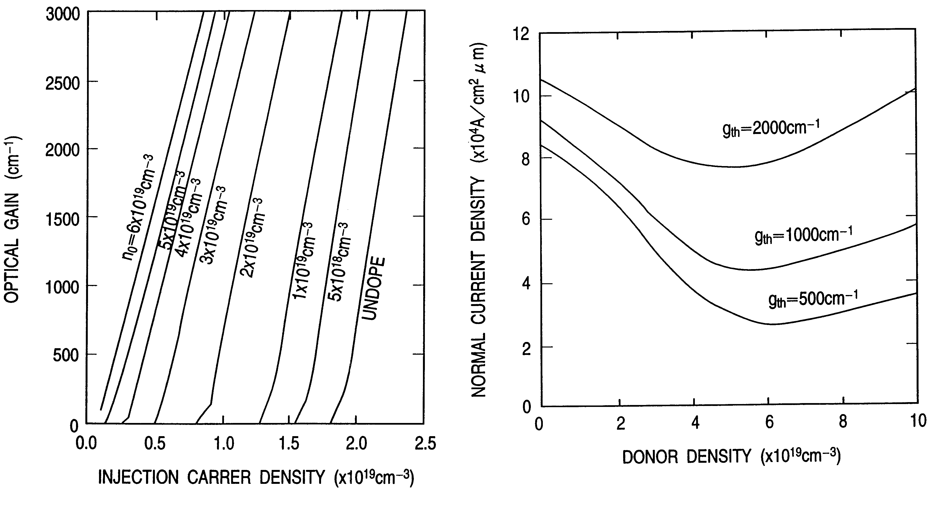
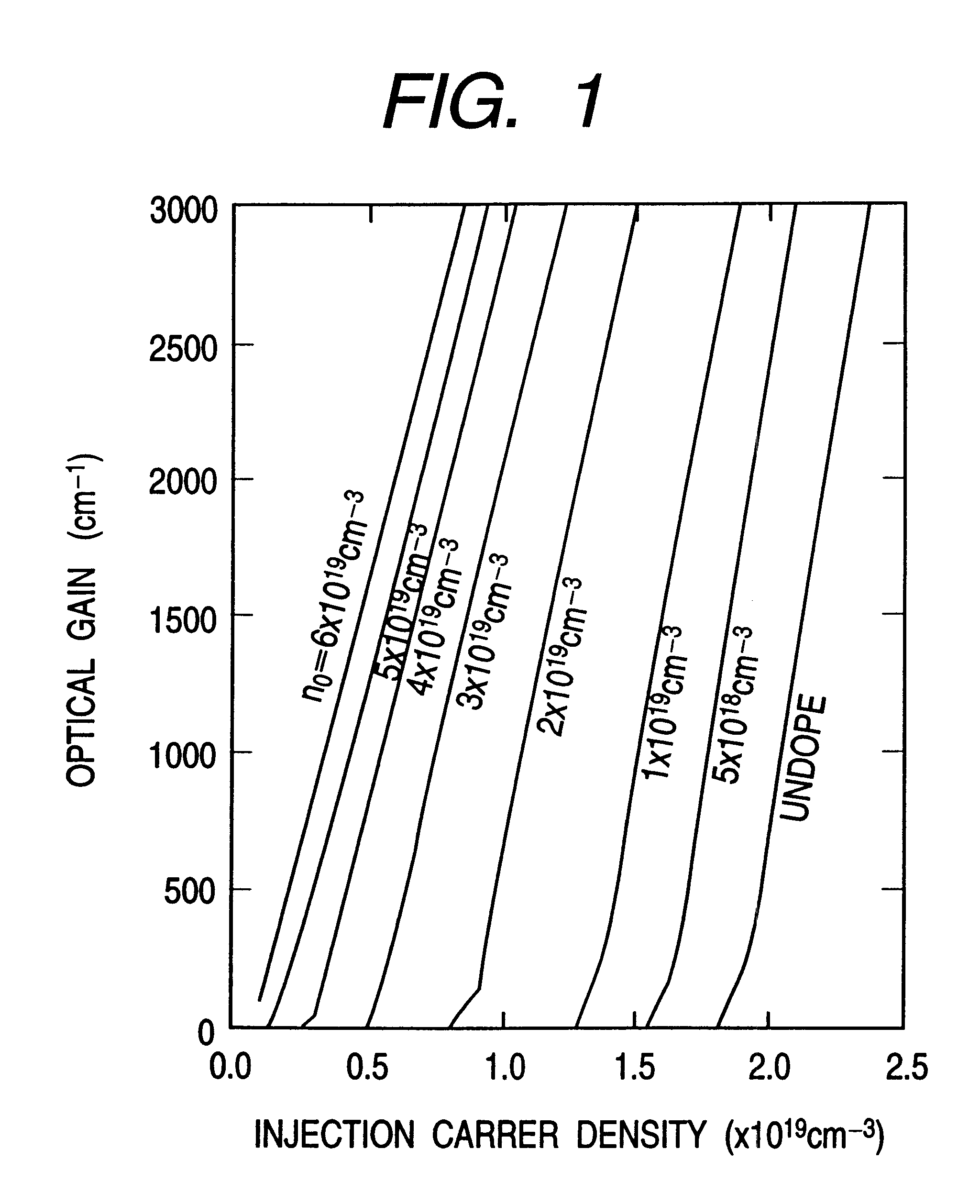
- Description
- Claims
- Application Information
AI Technical Summary
Benefits of technology
Problems solved by technology
Method used
Image

Examples
third example
FIG. 15 is a structural sectional view, taken from a plane crossing an optical axis, showing a semiconductor laser device as a third example of the present invention.
The semiconductor laser device having a multi-quantum well structure in this example is formed by sequentially stacking, on an n-type SiC substrate 51 with the (1,0,-1,0) plane taken as the principle plane thereof, a low temperature buffer layer 2 made from n-type GaN, a high temperature buffer layer 3 made from n-type GaN, an n-type Al.sub.0.2 Ga.sub.0.8 N cladding layer 4, an n-type GaN optical guide layer 5, a GaInN multi-quantum well active region 6, a p-type GaN optical guide layer 7, a p-type Al.sub.0.2 Ga.sub.0.8 N cladding layer 8, and a p-type GaN cap layer 9. Each of these layers (and region) is formed by epitaxial growth by the usual metal organic vapor phase epitaxial growth method. The thickness of each layer is set at 0.05 .mu.m (low temperature buffer layer 2), 3 .mu.m (high temperature buffer layer 3), 0...
second embodiment
One example of optical information processing equipment of a type making use of a state transition such as a phase transition of a recording medium will be described.
FIG. 16 is a basic configuration view showing one example of an optical disk apparatus. Reference numeral 211 designates a disk on which an optical recording medium for optical recording is provided; 212 is a motor for rotating the disk; 213 is an optical pickup; and 217 is a control unit for controlling these components. The optical pickup 213 has a lens system 214, a light source 215 such as a semiconductor laser device, and a photo detector 216.
The general configurations of such an optical disk apparatus have been variously reported, and therefore, only an important configuration will be briefly described. The optical disk apparatus is basically classified into a read-only type, a write once / read many times type, and rewritable type depending on the kind of a recording material.
The reproducing of information is perfo...
fourth example
A semiconductor laser device in this embodiment will be described with reference to FIG. 14.
The semiconductor laser device having a multi-quantum well structure in this example is formed by sequentially stacking, on a sapphire substrate 1 with the (1,0,-1,2) plane taken as the principle plane thereof, a low temperature buffer layer 2 made from n-type AlN, a high temperature buffer layer 3 made from n-type AlN, an n-type Al.sub.0.2 Ga.sub.0.8 N cladding layer 4, an n-type GaN optical guide layer 5, a GaInN multi-quantum well active region 6, a p-type GaN optical guide layer 7, a p-type Al.sub.0.2 Ga.sub.0.8 N cladding layer 8, and a p-type GaN cap layer 9. Each of these layers is formed by epitaxial growth by the usual metal organic vapor phase epitaxial growth method. The thickness of each layer is set at 0.05 .mu.m (low temperature buffer layer 2), 3 .mu.m (high temperature buffer layer 3), 0.3 .mu.m (n-type cladding layer 4), 0.1 .mu.m (n-type optical guide layer 5), 0.1 .mu.m (p-...
PUM
 Abstract
Description
Claims
Application Information