

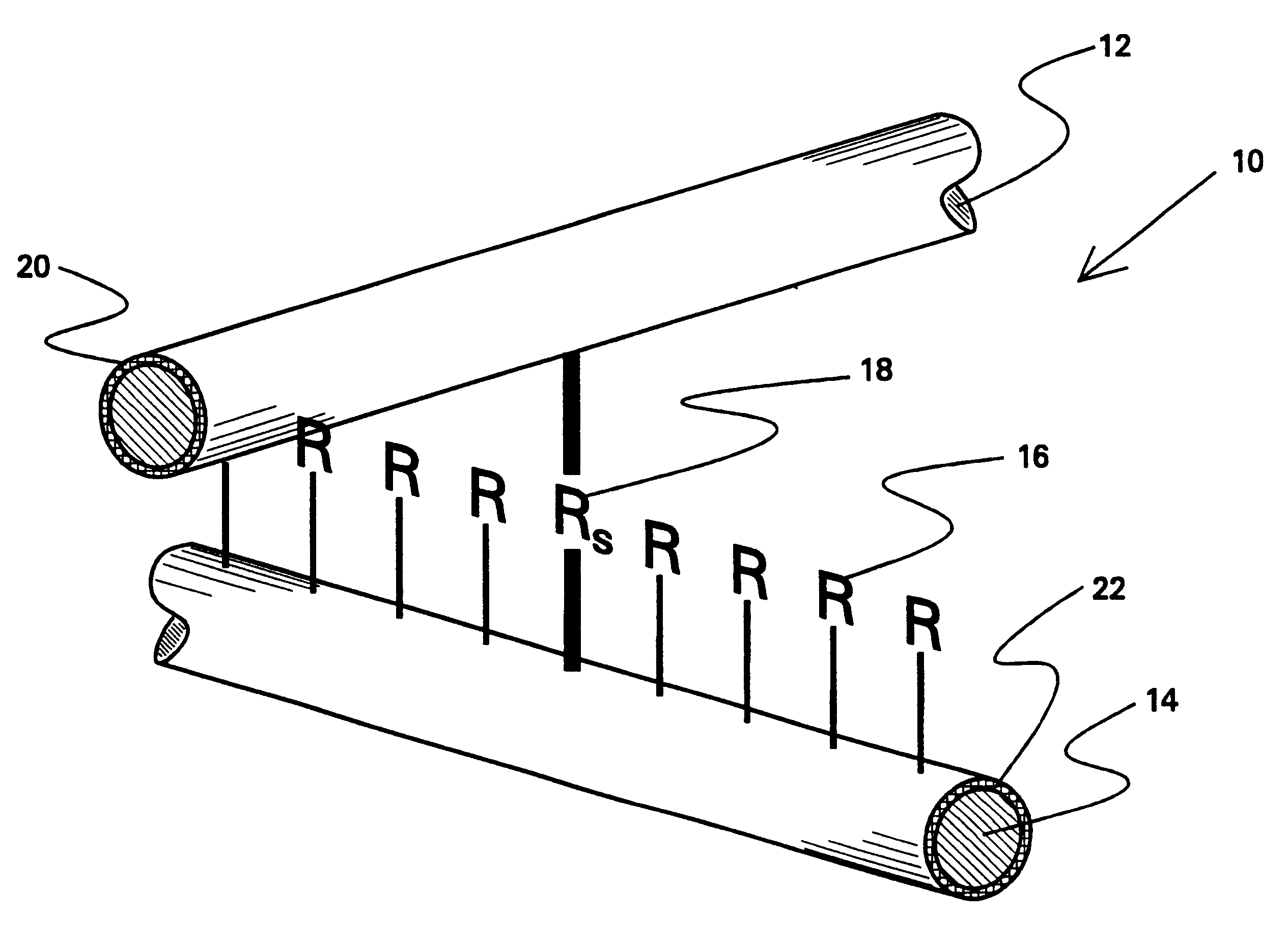
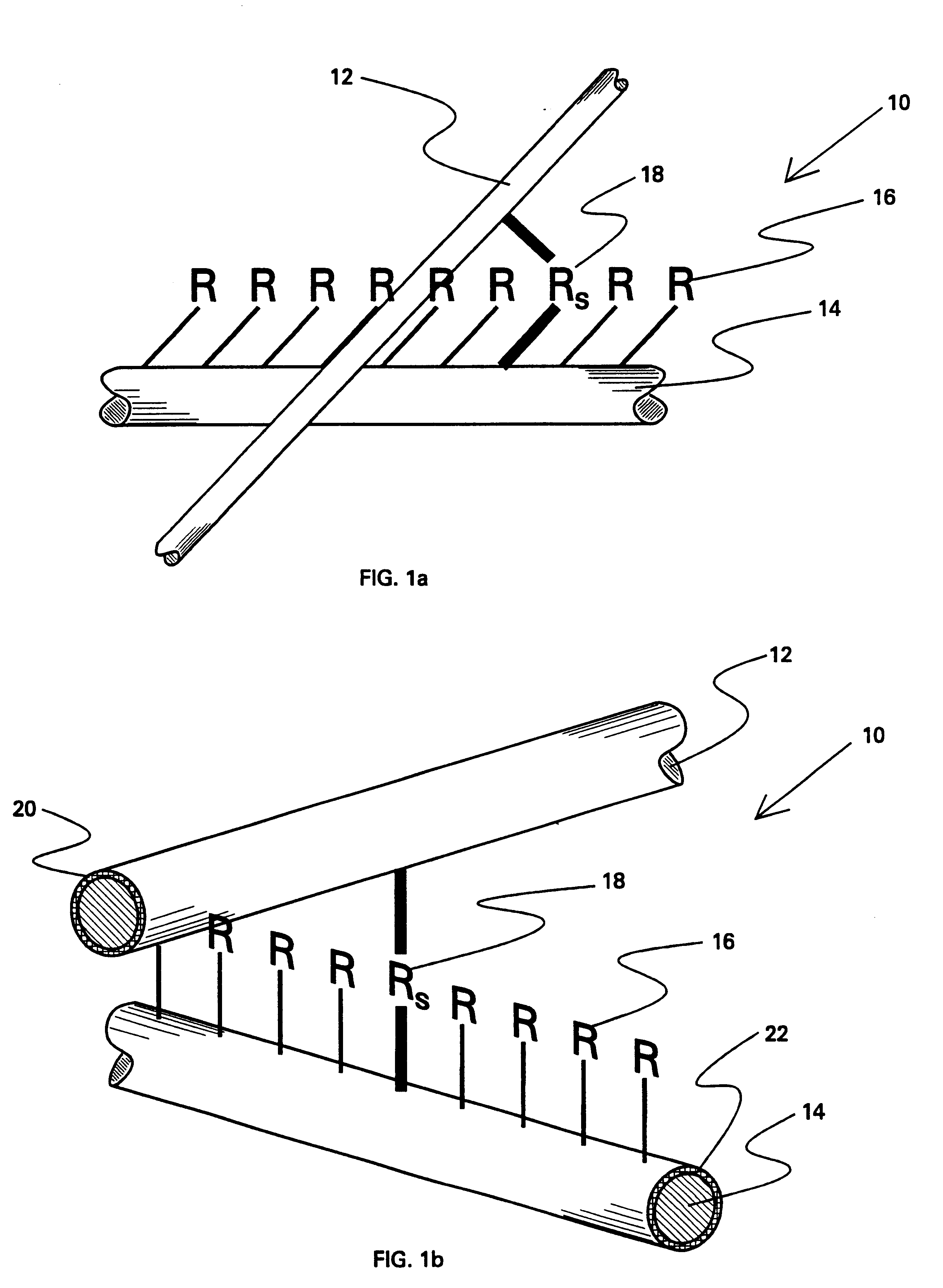
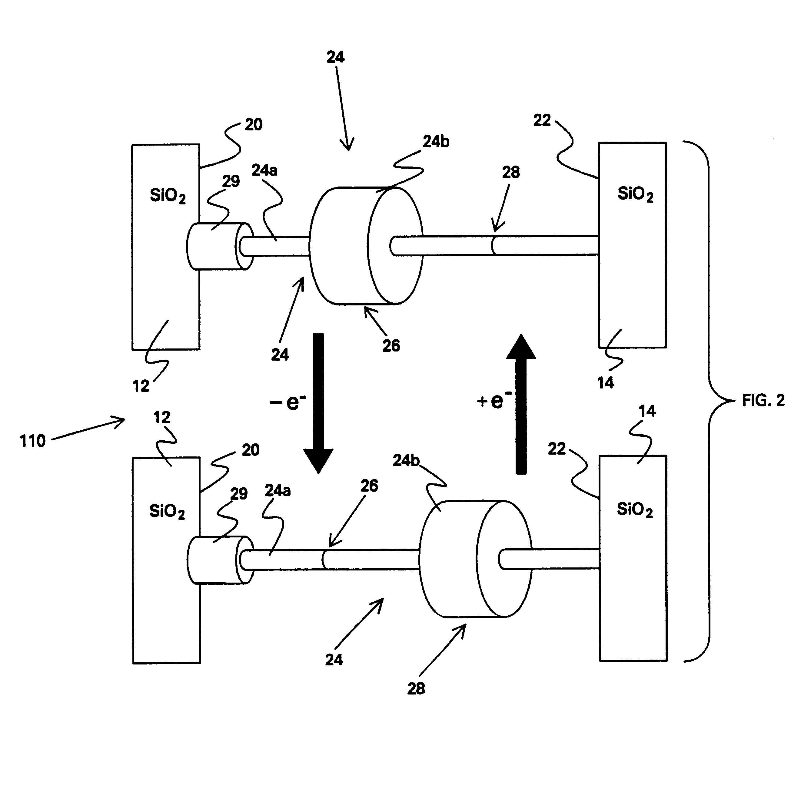
Molecular wire transistor (MWT)
- Summary
- Abstract
- Description
- Claims
- Application Information
AI Technical Summary
Benefits of technology
Problems solved by technology
Method used
Image

Examples
Embodiment Construction
Definitions
As used herein, the term "self-aligned" as applied to "junction" means that the junction that forms the switch and / or other electrical connection between two wires is created wherever two wires, either of which may be coated or functionalized, cross each other, because it is the act of crossing that creates the junction.
The term "self-assembled" as used herein refers to a system that naturally adopts some geometric pattern because of the identity of the components of the system; the system achieves at least a local minimum in its energy by adopting this configuration.
The term "singly configurable" means that a switch can change its state only once via an irreversible process such as an oxidation or reduction reaction; such a switch can be the basis of a programmable read only memory (PROM), for example.
The term "reconfigurable" means that a switch can change its state multiple times via a reversible process such as an oxidation or reduction; in other words, the switch can...
PUM
 Abstract
Description
Claims
Application Information