

Copper electroplating liquid, pretreatment liquid for copper electroplating and method of copper electroplating
- Summary
- Abstract
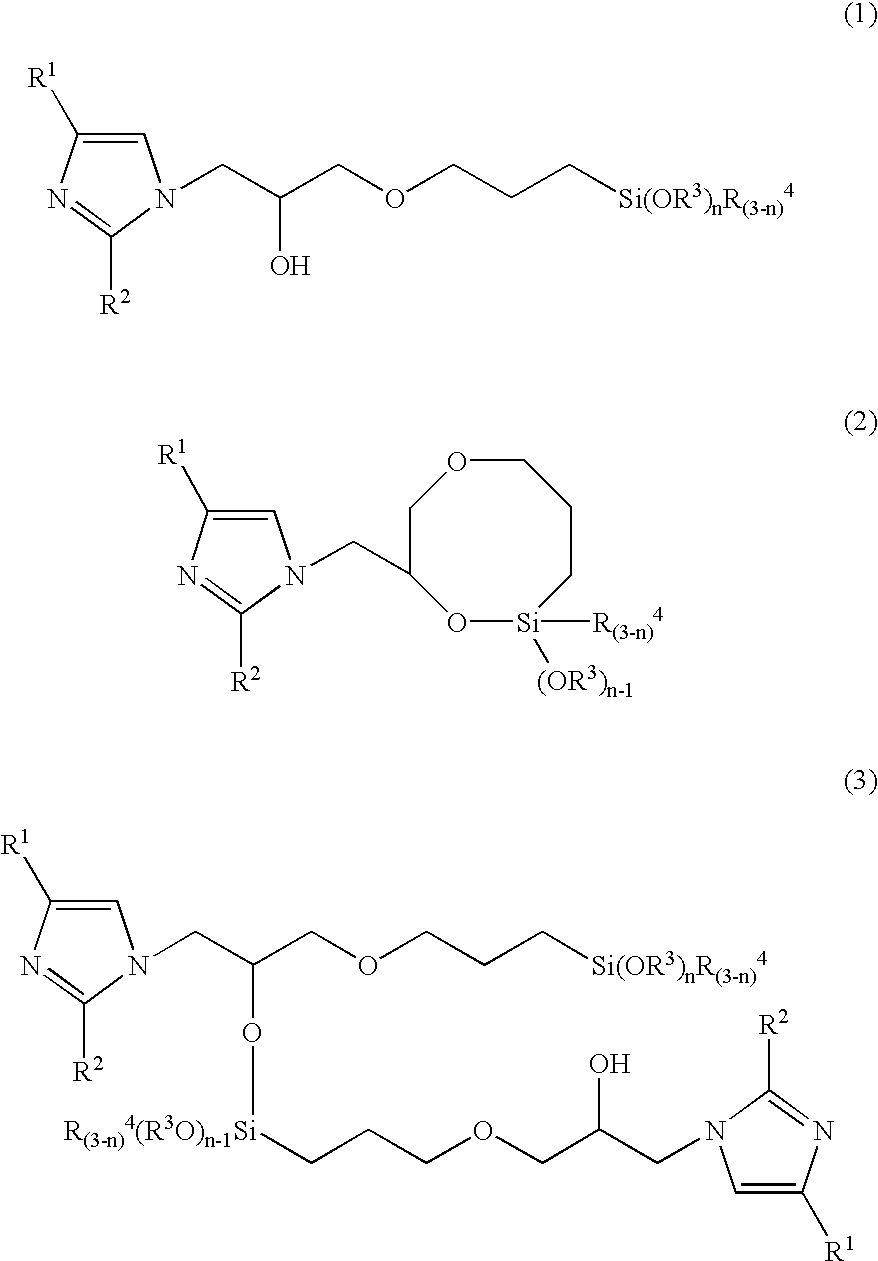
- Description
- Claims
- Application Information
AI Technical Summary
Benefits of technology
Problems solved by technology
Method used
Image

Examples
example 1
Copper 15 g / L, sulfuric acid 180 g / L, chlorine 70 mg / L, polyethyleneglycol (molecular weight: 3350) 50 .mu.mol / L, bis-(3-sulfopropyl) disulfide disodium salt 30 .mu.mol / L, quaternary epichlorohydrine (a quaternary ammonium salt addition compound consisting of a tertiary alkyl amine and polyepichlorohydrine) 6 .mu.mol / L, polybenzylethyleneimine 2 .mu.mol / L, an aqueous solution of imidazole silane (a mixed aqueous solution of 20 g / L of a silane coupling agent obtained by the equimolar reaction of imidazole and .gamma.-glycidoxypropyltrimethoxysilane or the like, and 20 mL / L of methanol) 50 mL / L
example 2
Copper 20 g / L, sulfuric acid 200 g / L, chlorine 50 mg / L, polyethyleneglycol (molecular weight: 10000) 10 .mu.mol / L, sodium 3-mercapto-1-propanesulfonate 30 .mu.mol / L, quaternary epichlorohydrine 30 .mu.mol / L, .gamma.-aminopropyltrimethoxysilane 2 g / L
example 3
Copper 30 g / L, sulfuric acid 180 g / L, chlorine 100 mg / L, polyethyleneglycol (molecular weight: 15000) 10 .mu.mol / L, bis-(2-sulfoethyl) disulfide disodium salt 20 .mu.mol / L, quaternary epichlorohydrine 15 .mu.mol / L, polyallylethyleneimine 1 .mu.mol / L, .gamma.-glycidoxypropyltriethoxysilane 500 mg / L
PUM
| Property | Measurement | Unit |
|---|---|---|
| Time | aaaaa | aaaaa |
| Time | aaaaa | aaaaa |
| Density | aaaaa | aaaaa |
Abstract
Description
Claims
Application Information