Structure for high speed printed wiring boards with multiple differential impedance-controlled layer

a technology of impedance control layer and structure, applied in the direction of printed element electric connection formation, high frequency circuit adaptation, etching metal masks, etc., can solve the problem that none of these addresses themselves directly to solving the problem

Inactive Publication Date: 2003-05-27
IBM CORP
View PDF12 Cites 26 Cited by
  • Summary
  • Abstract
  • Description
  • Claims
  • Application Information

AI Technical Summary

Benefits of technology

As described in the publication "Innovations in Base Materials and Polymer Applications", European Institute of Printed Circuits, 1994, this article merely discloses the impact on process yields of using a positive working ED resist so as to provide improved conductive contrast, resolution and conductive geometry in the construction of printed circuit boards.
Finally, the article "High Density MLB's With New Materials and Build-up Technologies", Printed Circuit World Convention VII Proceedings of May 1996 describe the utilization of new materials and the forming of multilayer laminates so as to provide improved innerlayer structures and buried via holes or blind via holes to resultingly improve higher density as well as higher accuracy in the electronic equipment and to also provide an environmentally-friendly enhanced printed circuit boards.
For instance, the application of the inventively produced structure of the printed wiring board with an IBM BT resin allows for a low loss, high speed printed wiring board utilization with excellent wiring density and signal integrity capabilities. The concept pertaining to the use of deep blind interconnect layering facilitates solutions to technical manufacturing problem in plating aspect ratio difficulties by allowing for the plating and controlled copper finishing on independently fabricated subcomposite structures, which are then combined through lamination into one contiguous printed wiring board structure with highly reproducible or controllable dielectric thickness and copper feature attributes. This processing control is vital in order to achieve the proper signal integrity which is required in order to meet high speed printed wiring board applications which are currently being developed and contemplated for future applications in the technology and industry.
Pursuant to the invention, by utilizing varying dielectric thicknesses or substrates in combination with controlled copper deposition and surface treatment to achieve the proper combination of thickness, spacing, copper line width thickness and all inner and outer layers, and conductive paste-filled blind and through vias., there is developed a structure which will simultaneously apply various types of impedance controlled innerlayers on a printed wiring board. The resulting structure thus utilizes a unique combination of existing and modified manufacturing processes in order to achieve the proper attributes, wherein lamination hole fill comprising conductive pastes, deep blind vias, conductive paste-filled drilled-through holes and subcomposite structures and controlled fluid head copper etch, such as through chemical polishing, may comprise key elements allowing for the economical manufacture of the printed wiring board.
Accordingly, it is a primary object of the present invention to provide a novel method for producing a printed wiring board structure which incorporates an improved impedance control.

Problems solved by technology

Although various types of multilayer and single-layer structures for printed wiring boards (PWB) and printed circuit boards (PCB) have been developed in the technology, none of these address themselves directly to solving the problem associated with the providing of tightly controlled impedances through structures and methods which will facilitate attainment of satisfactory levels of signal integrity.

Method used


Image

  • Structure for high speed printed wiring boards with multiple differential impedance-controlled layer
  • Structure for high speed printed wiring boards with multiple differential impedance-controlled layer
  • Structure for high speed printed wiring boards with multiple differential impedance-controlled layer

Examples


Embodiment Construction

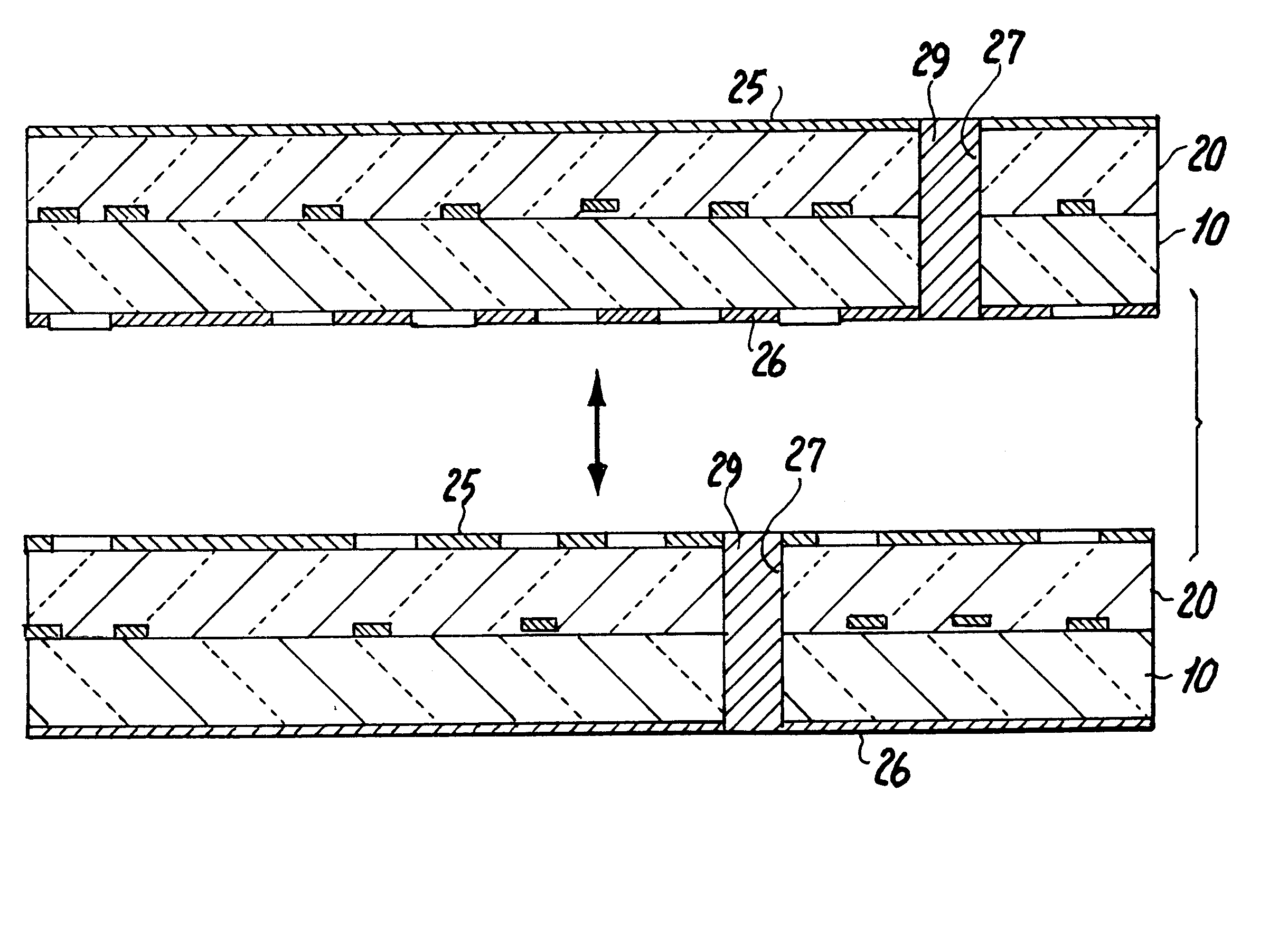
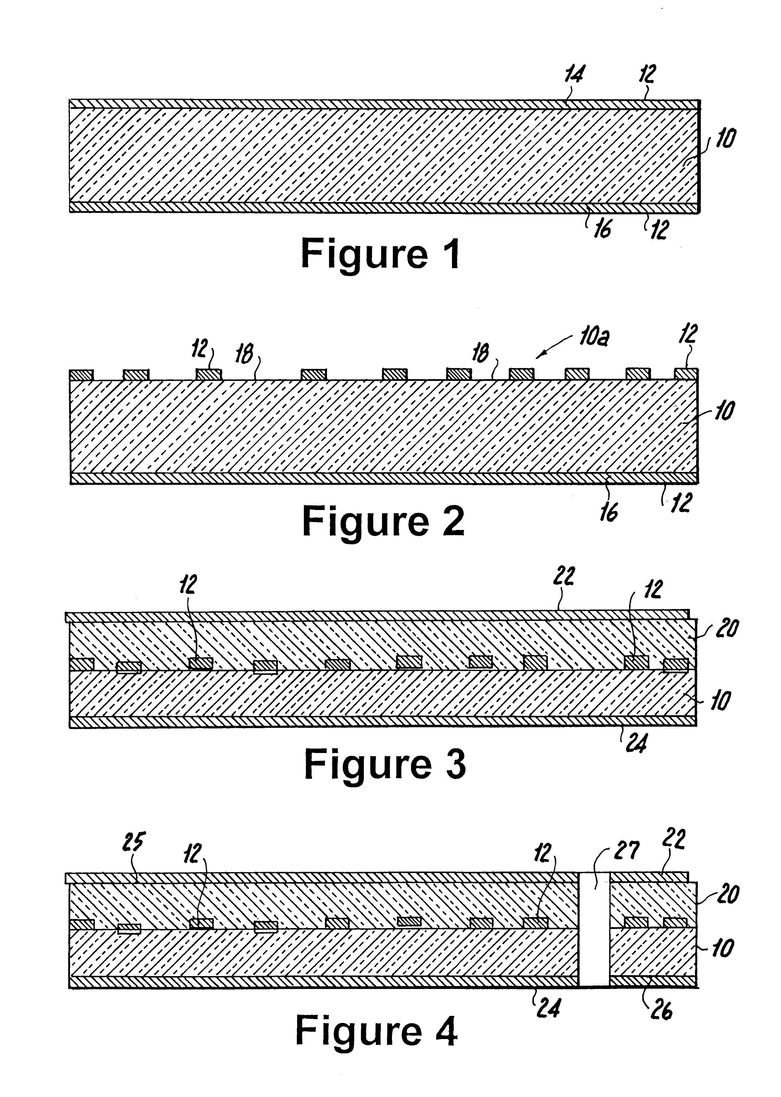
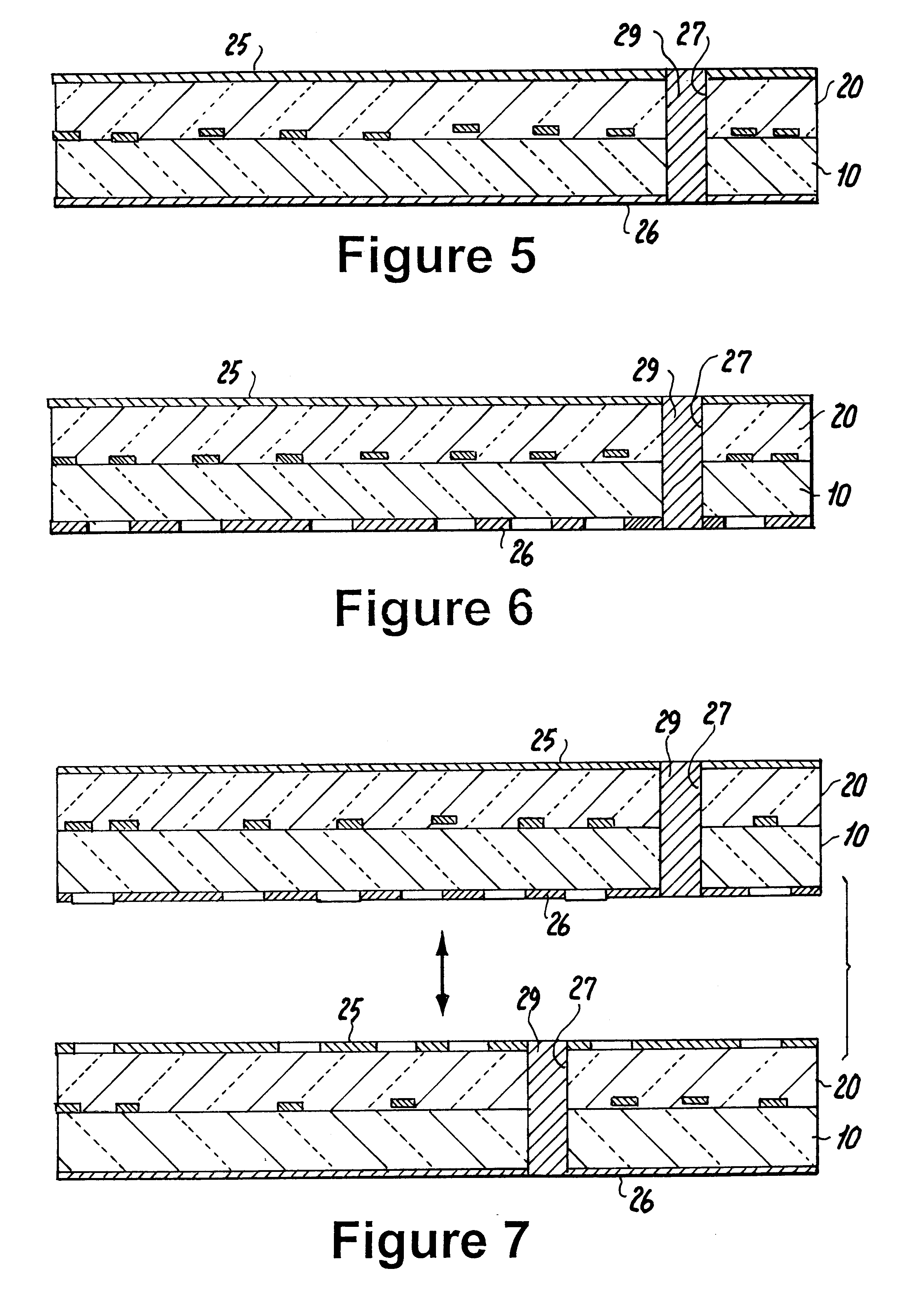
Referring in more specific detail to the drawings, particularly, FIG. 1 illustrates a section of a dielectric substrate 10 for a printed wiring board having a thickness of copper foil material 12 applied on both sides or surfaces 14, 16 thereof, in an initial step of producing the impedance controlled printed wiring board structure. Although two conductive layers and one dielectric layer are shown for base member 10, it is understood that the invention is not limited thereto. Specifically, it is only necessary to provide one such conductive layer and one such dielectric layer while still attaining the advantageous results taught herein. At least two layers of each are used when it is desired to incorporate an internal conductive plane (e.g., power, ground or signal) as part of the final structure. Understandably, several conductive dielectric layers and corresponding internal conductive planes may be utilized, depending on operational requirements for the finished product. Subsequen...


PUM

PropertyMeasurementUnit
aspect ratioaaaaaaaaaa
impedanceaaaaaaaaaa
thicknessaaaaaaaaaa

Abstract

A method and arrangement for creating an impedance controlled printing wiring board, particularly the formation of a structure for high speed printed wiring boards incorporating multiple differential impedance controlled layers. Furthermore, there are provided vias of either through-holes, blind holes and buried holes filled with a conductive paste material to form electrical interconnections with conductive layers of the printed wiring board.

Description

1. Field of the InventionThe present invention relates to a method for creating an impedance controlled printed wiring board. More particularly, the invention is directed to the formation of a structure for high speed printed wiring boards incorporating multiple differential impedance controlled layers. Furthermore, the invention is also directed to the provision of a method for producing an impedance controlled printed circuit wiring board. Moreover, the invention is further directed to the provision of a method for producing high speed printed wiring boards with multiple differential impedance controlled layers; especially with edge and broadside differentials.In essence, problems are encountered in the technology with regard to the production of printed wiring boards and which incorporate so-called deep blind vias while maintaining a tight and stringent impedance control.Presently, printed-wiring board (PWB) products which are intended for high frequency applications are provided...

Claims


Application Information

Patent Timeline
Patent Type & Authority Patents(United States)
IPC IPC(8): H01L23/58H01L23/48H01L23/498H01L23/66H05K3/40H05K3/46H05K1/02H05K3/24
CPCH01L23/49822H05K3/4069H05K3/4623H01L23/66Y10T29/4913H01L2924/3011H05K1/0237H05K3/246H05K3/4652H05K2201/0347H05K2201/0352H05K2201/0355H05K2203/0554H01L2924/0002H01L2924/00
Inventor MILLER, THOMAS RICHARDPAPATHOMAS, KONSTANTINOS I.CURCIO, BRIAN EUGENESNIEZEK, JOSEPH J.
Owner IBM CORP
Why Eureka
Try Eureka