

Field emission electron source and fabrication process thereof
- Summary
- Abstract
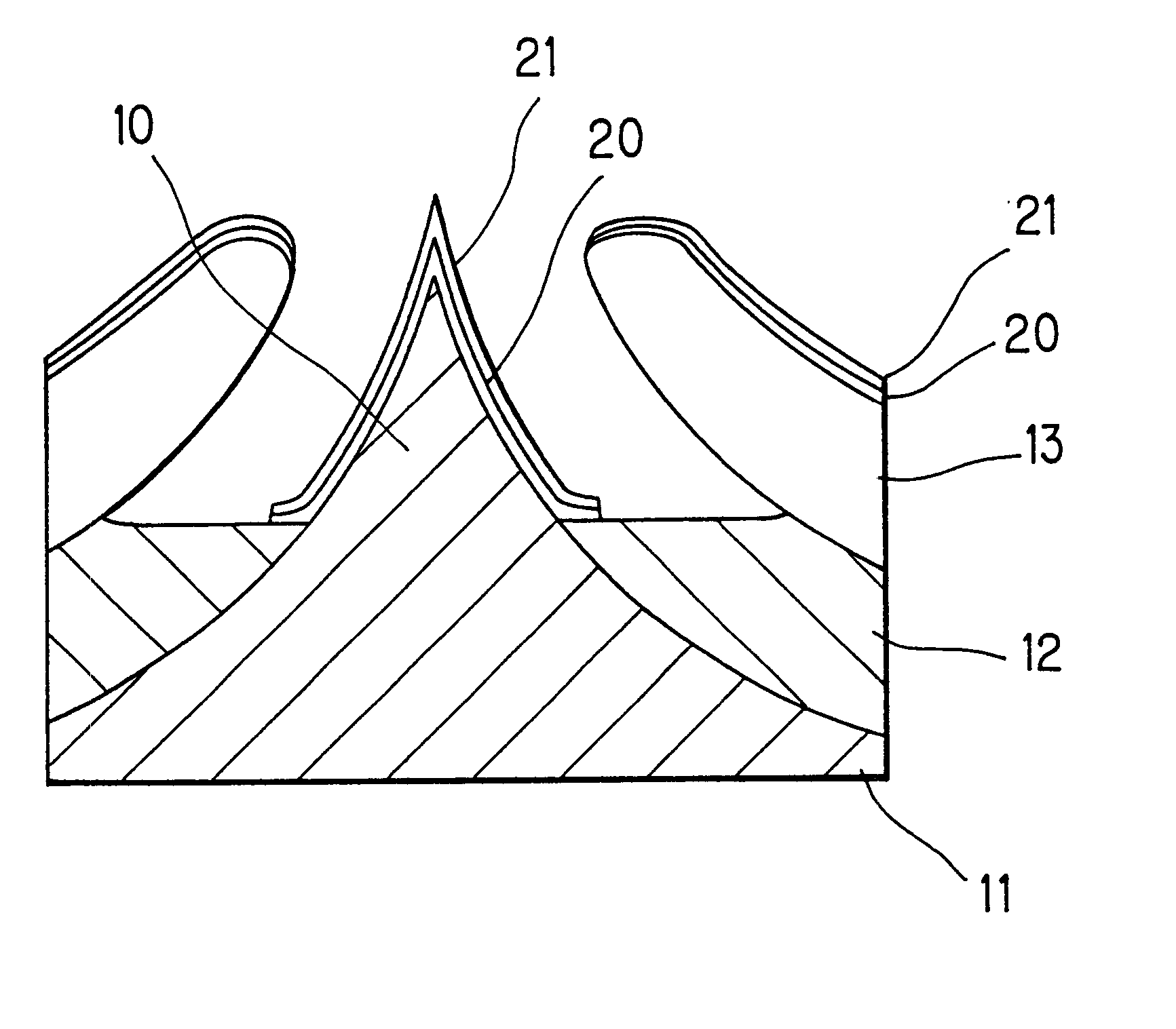
- Description
- Claims
- Application Information
AI Technical Summary
Problems solved by technology
Method used
Image

Examples
second example
(2) THE SECOND EXAMPLE
In this second example, a Mo coated silicon emitter shown in FIG. 5G was prepared in the same manner as the first example and then a film of ZrC which belongs to the same group as HfC was formed with a thickness of 3 nm as the second layer. The film was formed at a film forming rate of 0.25 nm / sec, at a substrate temperature of 200.degree. C. under a vacuum of 4.times.10.sup.-6 torr.
The device thus formed was set under a ultra-high vacuum (5.times.10.sup.-9 torr) and the emission current was measured in a triode arrangement. With a gate voltage of 100 V, a current exceeding 100 .mu.A was confirmed. The effective work function .PHI. determined based on the obtained F-N curve and the diameter at the device tip measured by a high-resolution electron microscope was 2.9 eV (.PHI.=2.9 eV) with the tip diameter of 9 nm.
third example
(3) THE THIRD EXAMPLE
In the third example, a silicon emitter shown in FIG. 5F was prepared in the same manner as the first example and then W instead of Mo was deposited as the first layer. Tungsten was selected because it belongs to the same group as Mo, has a relatively similar physical properties and hence is considered to have the same effects as Mo. In this example, a film of 10 nm was formed in the same manner by EB vapor deposition. The film was formed at a film forming rate of 0.2 nm / sec, at a substrate temperature of 200.degree. C. under a vacuum of 5.times.10.sup.-6 torr.
Then, a HfC film was formed of 3 nm thick as the second layer in the same manner as the first example. The film was formed at a film forming rate of 0.25 nm / sec, at a substrate temperature of 200.degree. C. under a vacuum of 5.times.10.sup.-6 torr. The device thus formed was set under a ultra-high vacuum (5.times.10.sup.-9 torr) and the emission current was measured in a triode arrangement. With a gate vol...
fourth example
(4) THE FOURTH EXAMPLE
In the fourth example, a W-coated silicon emitter shown in FIG. 5G was prepared in the same manner as the third example and then a film of ZrC which belongs to the same group was formed of 3 nm thick as the second layer. The film was formed at a film forming rate of 0.25 nm / sec, at a substrate temperature of 200.degree. C. under a vacuum of 4.times.10.sup.-6 torr. The device thus formed was set under a ultra-high vacuum (5.times.10.sup.-9 torr) and the emission current was measured in a triode arrangement. With a gate voltage of 100 V, a current exceeding 150 .mu.A was confirmed. The effective work function .PHI. determined based on the obtained F-N curve and the diameter at the device tip measured by a high-resolution electron microscope was 3.0 eV (.PHI.=3.0 eV) with the tip diameter of 9 nm.
Although no detailed description is given as to the first through fourth examples, the film thickness is 5 nm minimum for the first layer and 3 nm minimum for the second ...
PUM
 Abstract
Description
Claims
Application Information