Dual-gate CMOS semiconductor device manufacturing method

a semiconductor device and manufacturing method technology, applied in semiconductor devices, semiconductor/solid-state device details, electrical devices, etc., can solve problems such as disadvantageous degradation of semiconductor devices

Inactive Publication Date: 2003-08-05
LAPIS SEMICON CO LTD
View PDF8 Cites 17 Cited by
  • Summary
  • Abstract
  • Description
  • Claims
  • Application Information

AI Technical Summary

Benefits of technology

According to the above-stated invention, the first conductive layer on the PMOS part and the first conductive layer on the NMOS part are isolated from each other by the formation of the groove region. It is, therefore, possible to reduce the mutual diffusion of the P type impurities and the N type impurities in the polycrystalline silicon layers.
The above-stated invention can provide a semiconductor device wherein the first conductive layer on the PMOS part is isolated from the first conductive layer on the NMOS part by a boundary portion. As a result, it is possible to reduce the mutual diffusion of the P type impurities and the N type impurities in the polycrystalline silicon layers through the first conductive layers.

Problems solved by technology

In other words, N type impurities are introduced into the polycrystalline silicon layer on the PMOS part and P type impurities are introduced into the polycrystalline silicon layer on the NMOS part, with the result that the performance of the semiconductor device disadvantageously deteriorates.

Method used


Image

  • Dual-gate CMOS semiconductor device manufacturing method
  • Dual-gate CMOS semiconductor device manufacturing method
  • Dual-gate CMOS semiconductor device manufacturing method

Examples


first embodiment

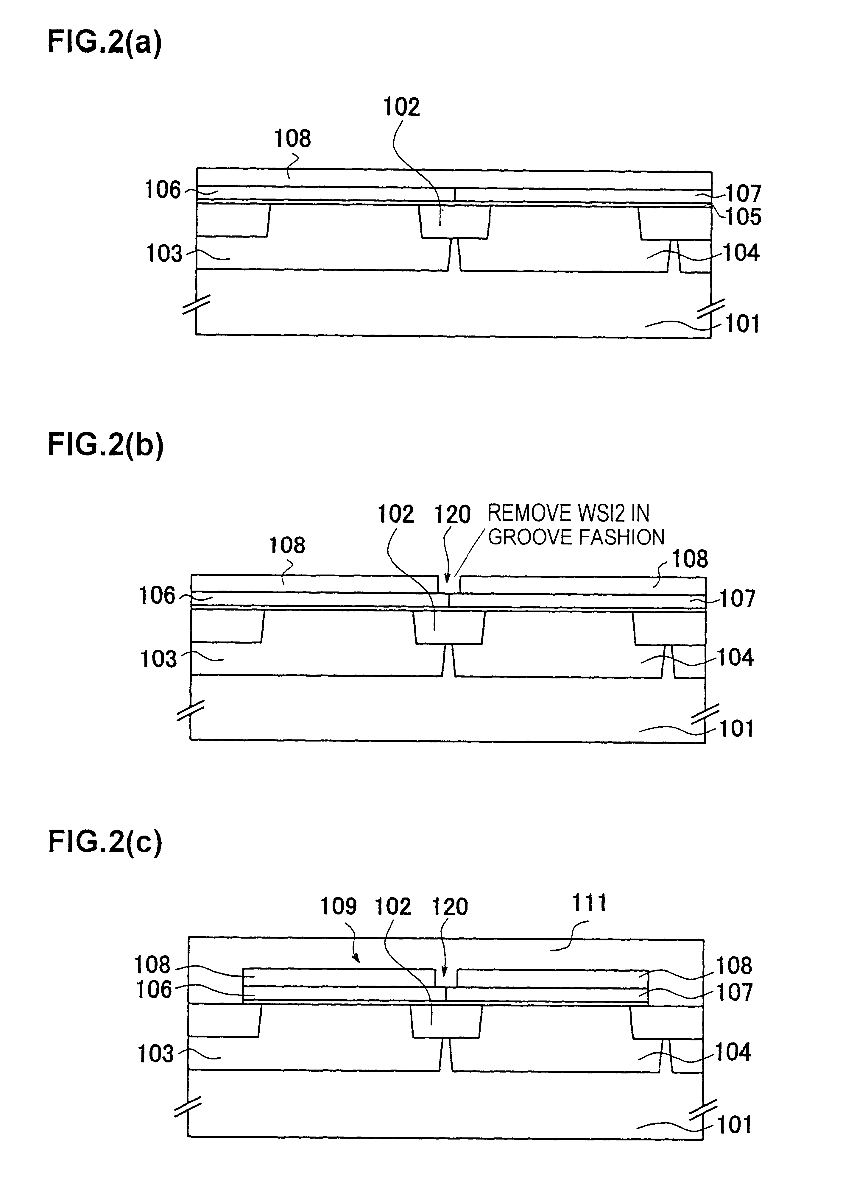
In the first embodiment, differently from the conventional semiconductor device, a groove region is formed in a WSi2 layer (or tungsten silicide layer) on a boundary region between an NMOS part and a PMOS part to thereby isolate the WSi2 layer on the NMOS part from the WSi2 layer on the PMOS part.

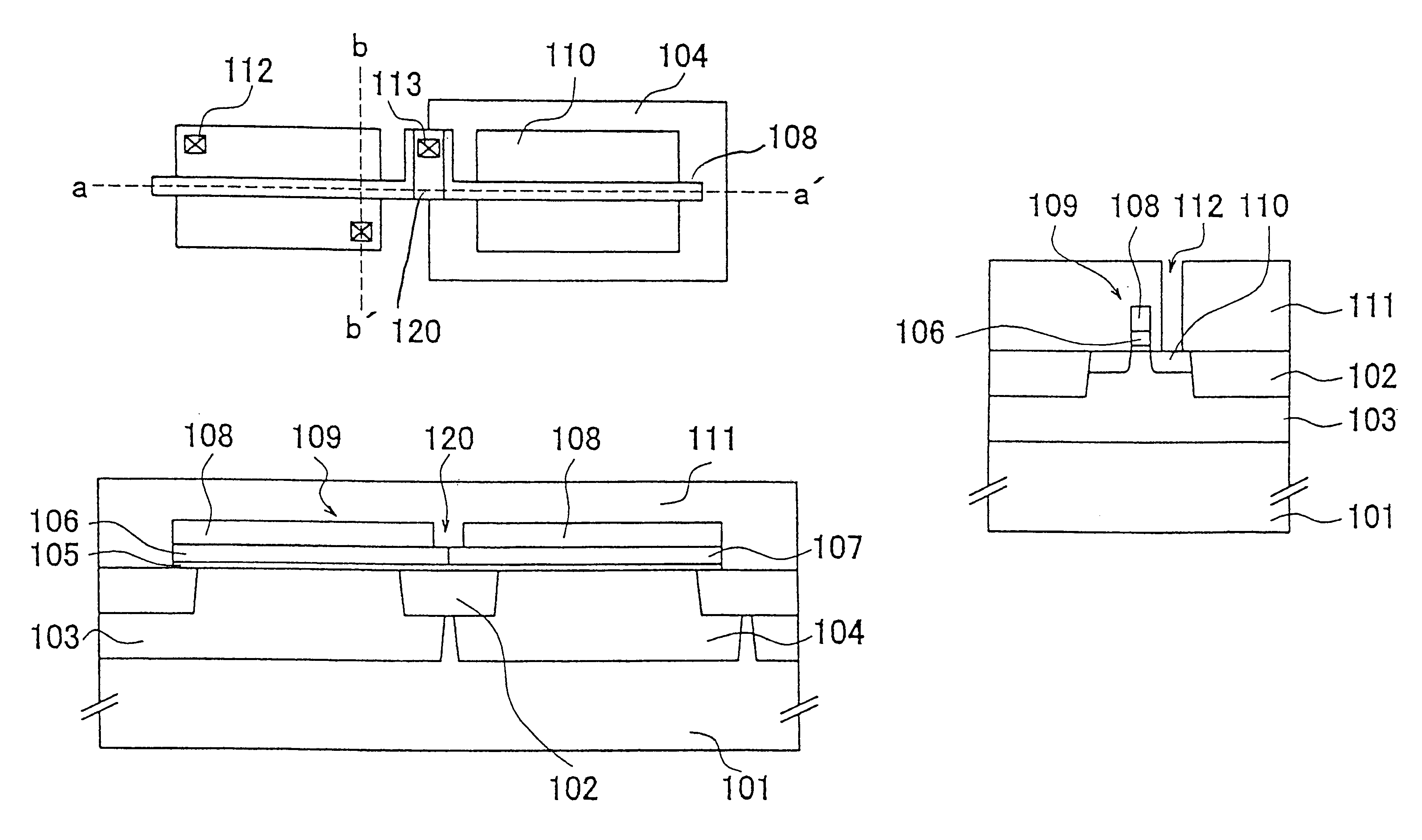
The constitution of a semiconductor device in the first embodiment will be described with reference to FIG. 1. FIG. 1A is a top view showing the constitution of the semiconductor device in the first embodiment. FIG. 1B is a cross-sectional view taken along line a-a' of FIG. 1A, showing the constitution of the semiconductor device in this embodiment. FIG. 1C is a cross-sectional view taken along line b-b' of FIG. 1A, showing the constitution of the semiconductor device in this embodiment.

First, as shown in FIG. 1, an element isolation insulating film 102 is formed on a silicon substrate 101 by, for example, an STI method. Impurities are injected into an NMOS part and a PMOS part by a photoli...

second embodiment

In the first embodiment stated above, description has been given to a case where the groove region is formed in the WSi2 layer on the boundary region between the NMOS part and the PMOS part and where the WSi2 layer on the NMOS part and the WSi2 layer on the PMOS part are isolated from each other. In the second embodiment, a CoSi2 layer (or cobalt silicide layer) having a low impurity diffusion coefficient and high conductivity is formed on a polycrystalline silicon layer on the bottom of a groove region on the first conductive layer.

Now, the constitution of a semiconductor device in the second embodiment will be described with reference to FIG. 3. FIG. 3A is a top view showing the constitution of the semiconductor device in the second embodiment. FIG. 3B is a cross-sectional view taken along line a-a' of FIG. 3A, showing the constitution of the semiconductor device in this embodiment. FIG. 3C is a cross-sectional view taken along line b-b' of FIG. 3A, showing the constitution of the...

third embodiment

In the first embodiment stated above, description has been given to a case where the groove region is formed in the WSi2 layer on the boundary region between the NMOS part and the PMOS part and where the WSi2 layer on the NMOS part and the WSi2 layer on the PMOS part are isolated from each other. In the third embodiment, an oxide film almost equal in height to a WSi2 layer is formed in a groove region.

Now, referring to FIG. 5, the constitution of a semiconductor device in the third embodiment will be described. FIG. 5A is a top view showing the constitution of the semiconductor device in the third embodiment. FIG. 5B is a cross-sectional view taken along line a-a' of FIG. 5A. FIG. 5C is a cross-sectional view taken along line b-b' of FIG. 5A.

First, as shown in FIG. 5, an element isolation insulating film 302 is formed on a silicon substrate 301 by, for example, the STI method. Impurities are injected into an NMOS part and a PMOS part by the photolithographic method and the implantat...


PUM

PropertyMeasurementUnit
insulatingaaaaaaaaaa
conductiveaaaaaaaaaa
heightaaaaaaaaaa

Abstract

A manufacturing method for a dual-gate CMOS semiconductor device that suppresses mutual diffusion of P type impurities and N type impurities in a gate electrode. An NMOS part and a PMOS part are formed on a semiconductor substrate. A polycrystalline silicon layer is formed on the NMOS part and the PMOS part, and consists of an N type impurity containing polycrystalline silicon layer and a P type impurity containing polycrystalline silicon layer. A first conductive layer is formed on the polycrystalline silicon layer so as to include a groove region, in which the first conductive layer is not formed, on a predetermined region including a boundary between the N type impurity containing polycrystalline silicon layer and the P type impurity containing polycrystalline silicon layer.

Description

1. Field of the InventionThe present invention relates to a dual-gate CMOS semiconductor device and a dual-gate CMOS semiconductor device manufacturing method. More specifically, the present invention relates to a dual-gate CMOS semiconductor device and a dual-gate CMOS semiconductor device manufacturing method capable of reducing the mutual diffusion of impurities in a gate electrode.2. Description of Related ArtIn recent years, CMOS semiconductor devices of a dual-gate structure have been adopted with a view of improving performance and reducing power consumption. As the gate electrodes of this dual-gate structure, a polycrystalline silicon layer containing N type impurities such as arsenic is used on an NMOS part and a polycrystalline silicon layer containing P type impurities such as boron is used on a PMOS part.The semiconductor device of such a dual-gate structure is disclosed by, for example, "M. Togo, et al., Thermal Robust Dual-Gate CMOs Integration Technologies for High-Pe...

Claims


Application Information

Patent Timeline
Patent Type & Authority Patents(United States)
IPC IPC(8): H01L21/70H01L21/8238H01L21/28H01L21/265H01L21/3205H01L21/768H01L23/52H01L23/522H01L27/092
CPCH01L21/823842H01L21/823871
Inventor TANAKA, HIROYUKI
Owner LAPIS SEMICON CO LTD
Why Eureka
Try Eureka