Semiconductor laser, semiconductor device, and their manufacture methods

a semiconductor and laser technology, applied in semiconductor lasers, laser details, electrical equipment, etc., can solve the problems of high manufacturing cost, hard to generate cracks in the algan buffer layer, and difficult to generate cracks in the buffer region

Inactive Publication Date: 2003-08-12
FUJITSU LTD
View PDF8 Cites 105 Cited by
  • Summary
  • Abstract
  • Description
  • Claims
  • Application Information

AI Technical Summary

Problems solved by technology

With this manufacture method, although the dislocation density of the GaN buffer layer can be lowered, the number of processes increases so that the manufacture cost rises.
The resonator side surfaces are formed by dry etching because it is difficult to cleave a sapphire substrate.
As compared to covering the whole substrate surface with the buffer

Method used


Image

  • Semiconductor laser, semiconductor device, and their manufacture methods
  • Semiconductor laser, semiconductor device, and their manufacture methods
  • Semiconductor laser, semiconductor device, and their manufacture methods

Examples


first embodiment

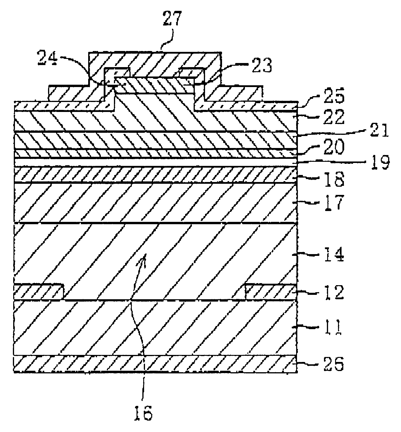
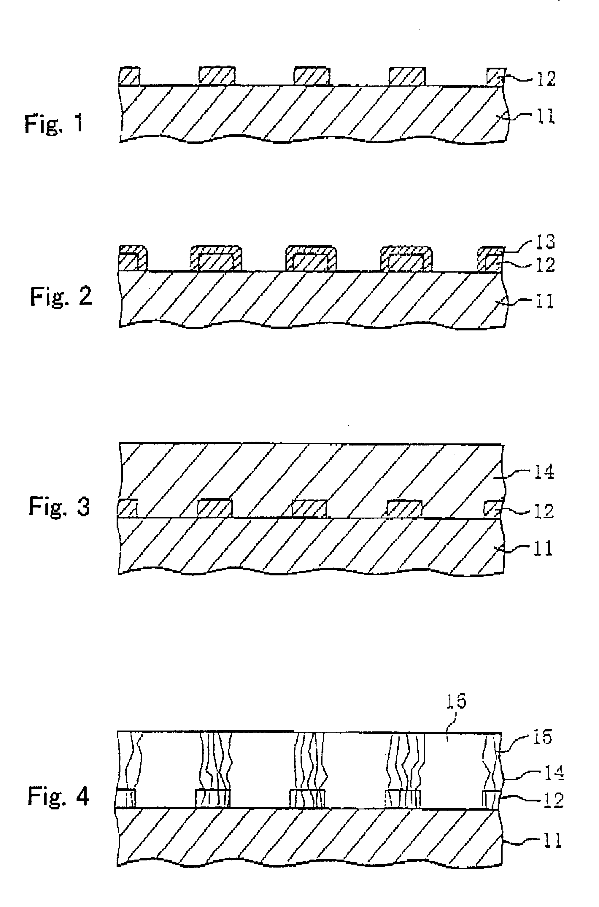
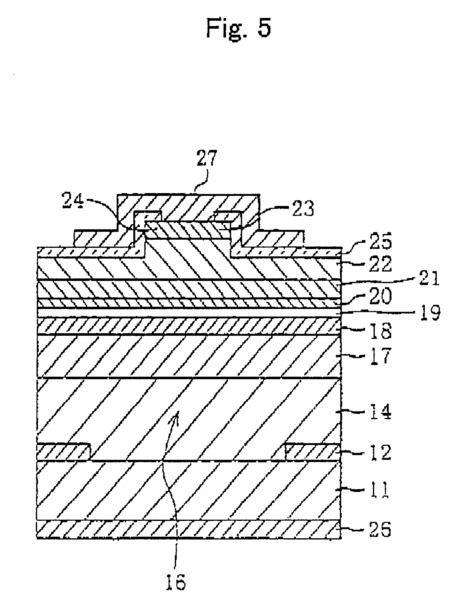
With reference to FIGS. 1 to 5, a method of manufacturing a semiconductor laser according to the invention will be described.

As shown in FIG. 1, a SiC substrate 11 having a (0001) Si plane as its principal surface is cut from a hexagonal 6H-SiC bulk grown by an improved Rayleigh method. The SiC substrate 11 is doped with n-type impurities at a carrier concentration of 2.times.10.sup.18 cm.sup.-3.

On the SiC substrate, an n-type Al.sub.0.1 Ga.sub.0.9 N layer is grown having an impurity concentration of 8.times.10.sup.18 cm.sup.-3 and a thickness of 100 nm. The thickness may be 50 to 300 nm and the impurity concentration may be 5.times.10.sup.17 to 1.times.10.sup.19 cm.sup.-3. This AlGaN layer is grown by MOVPE. For example, trimethylgallium (TMGa), trimethylaluminum (TMAI) and ammonia are used as source gas, SiH.sub.4 is used as source dopant and hydrogen is used as carrier gas. The growth conditions are a pressure of 100 Torr and a temperature of 1090.degree. C. The pressure may be 7...

second embodiment

Next, with reference to FIGS. 6 to 9, the method of manufacturing a semiconductor laser will be described.

An SiC substrate 11 shown in FIG. 6 is similar to the SiC substrate 11 of the first embodiment shown in FIG. 1 An SiO.sub.2 film is formed on the surface of the SiC substrate 11 to a thickness of 200 nm by thermal chemical vapor deposition (thermal CVD). The thickness of the SiO.sub.2 film may be set to 100 to 500 nm. This SiO.sub.2 film is selectively etched by using hydrofluoric acid to leave striped SiO.sub.2 masks 28.

The width of the SiO.sub.2 mask 28 is 4.0 .mu.m and a distance (pitch) between centers of adjacent SiO.sub.2 masks 28 is 8.0 .mu.m. The SiO.sub.2 mask width may be set to 1.0 to 10.0 .mu.m and the pitch may be set to 2.0 to 20.0 .mu.m.

As shown in FIG. 7, an n-type Al.sub.0.1 Ga.sub.0.9 N layer 12 having a thickness of 100 nm and an impurity concentration of 8.times.10.sup.18 cm.sup.-3 is selectively grown on the exposed surface of the SiC substrate 11. The thic...

third embodiment

Next with reference to FIGS. 10 and 11, the third embodiment will be described.

As shown in FIG. 10, on the surface of an n-type SiC substrate 11, an n-type AlGaN pattern 29 is formed. The SiC substrate 11 is similar to the SiC substrate of the first embodiment shown in FIG. 1. The n-type AlGaN pattern 29 is formed by a method similar to that used for forming the AlGaN pattern 12 of the first embodiment shown in FIG. 1. Although the AlGaN pattern 12 shown in FIG. 1 is parallel to the direction of the SiC substrate 11, the AlGaN pattern 29 of the second embodiment is parallel to the direction of the SiC substrate 11. The AlGaN pattern 29 has a thickness of 100 nm, a width of 4.0 .mu.m, a pitch of 8.0 .mu.m and an impurity concentration of 8.times.10.sup.18 cm.sup.-3. The pattern may be set so that it has the thickness of 50 to 300 nm, the width of 1.0 to 10.0 .mu.m, the pitch of 20 to 20.0 .mu.m and the impurity concentration of 5.times.10.sup.17 to 1.times.10.sup.19 cm.sup.-3.

By us...


PUM


Abstract

A substrate is made of SiC. A plurality of AlxGa1-xN patterns (0<=x<=1) is formed on a surface of the substrate and dispersively distributed in an in-plane of the substrate. An AlyGa1-yN buffer layer (0<=y<=1) covers the surface of the substrate and the AlxGa1-xN patterns. A laser structure is formed on the AlyGa1-yN buffer layer. Since the AlGaN buffer layer is grown by using the AlGaN patterns as seed crystals, a dislocation density of a predetermined region in the AlGaN buffer layer can be lowered. The characteristics of a laser structure can be improved by forming the laser structure above the region having a low dislocation density. Since the AlGaN pattern has electric conductivity, the device resistance can be suppressed from being increased.

Description

The present invention relates to a semiconductor laser, a semiconductor device and their manufacture methods, and more particularly to a semiconductor laser and a semiconductor device having a semiconductor region of a low dislocation density, and to their manufacture methods.DESCRIPTION OF THE RELATED ARTActive developments on light emitting devices using GaN based materials are being made nowadays. Blue and green high luminance light emitting diodes (LED) have been manufactured to date. Oscillation of a royal purple laser at a room temperature has been realized by many research organizations including the present inventor, and studies of manufacturing the products of this laser are made vigorously. A GaN based laser using a sapphire (Al.sub.2 O.sub.3) substrate was manufactured and continuous wave oscillation (CW oscillation) during 1000 hours was confirmed (refer to S. Nakamura et al., Japanese Journal of Applied Physics, vol. 35, p. L74, 1996).A manufacture method for a short wa...

Claims


Application Information

Patent Timeline
IPC IPC(8): H01S5/32H01S5/323H01S5/00H01S5/02
CPCH01S5/32H01S5/32341H01S5/021H01S5/3201H01S5/3226H01S2304/12H01S5/2206
Inventor KURAMATA, AKITOHORINO, KAZUHIKO
Owner FUJITSU LTD
Why Eureka
Try Eureka