Silicon on insulator field effect transistors having shared body contact

a technology of field effect transistors and insulators, which is applied in the field of silicon on insulator field effect transistors having shared body contact, very large scale integrated circuits, etc., can solve the problems of unintentionally inducing local body effects in some cell devices, sporadic read upsets without apparent reason, and serious design problems, so as to improve memory cell stability

Inactive Publication Date: 2003-09-23
INT BUSIENSS MACHINES IBM +1
View PDF4 Cites 105 Cited by
  • Summary
  • Abstract
  • Description
  • Claims
  • Application Information

AI Technical Summary

Benefits of technology

It is a purpose of this invention i

Problems solved by technology

This trapped charge can produce unwanted device channel bias resulting in what is referred to as body effects that are localized to an individual device.
However, these localized body effects and other sporadically occurring parasitic bipolar effects, i.e., at source/drain diffusion junctions, are serious design problems for densely packed SOI circuits such as for example, memory arrays.
Repetitively accessing a random access memory (RAM) cell, both to read and to write it, unintentionally induces local body effects in some cell devices.
These local effects can ca

Method used


Image

  • Silicon on insulator field effect transistors having shared body contact
  • Silicon on insulator field effect transistors having shared body contact
  • Silicon on insulator field effect transistors having shared body contact

Examples


Embodiment Construction

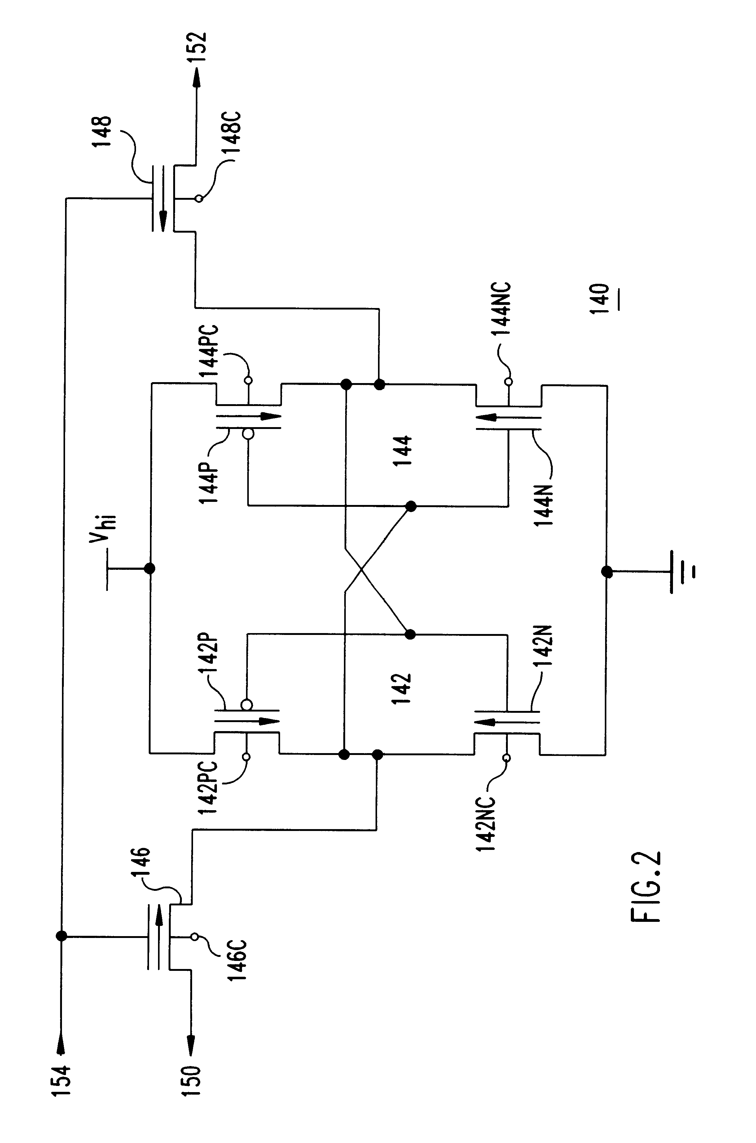
Turning now to the drawings and, more particularly, FIG. 2 is a schematic of a typical CMOS Static RAM (SRAM) cell 140. The cell 140 is, essentially, an identical pair of cross coupled CMOS inverters 142, 144 and a pair of pass transistors 146, 148 between the cross coupled inverters 142, 144 and a pair of bit lines 150, 152. A word line 154 is tied to the gate of pass transistors 146, 148. Each CMOS inverter 142, 144 is, simply, an NFET 142N, 144N and a PFET 142P, 144P. The gate and drain of each PFET 142P, 144P is tied to the gate and drain of corresponding NFET 142N, 144N, respectively. The source of the PFETs 142P, 144P are connected to supply voltage (V.sub.hi) and the source of the NFETs 142N, 144N are connected to GND. The channel body for each FET 142N, 142P, 144N, 144P, 146 and 148 is represented by node 142NC, 142PC, 144NC, 144PC, 146C and 148C, respectively. The state of the cross coupled inverter pair 142, 144 determines the state of data stored in the cell 140.

Each SRAM...


PUM


Abstract

Silicon on insulator (SOI) field effect transistors (FET) with a shared body contact, a SRAM cell and array including the SOI FETs and the method of forming the SOI FETs. The SRAM cell has a hybrid SOI/bulk structure wherein the source/drain diffusions do not penetrate to the underlying insulator layer, resulting in a FET in the surface of an SOI layer with a body or substrate contact formed at a shared contact. FETs are formed on SOI silicon islands located on a BOX layer and isolated by shallow trench isolation (STI). NFET islands in the SRAM cells include a body contact to a P-type diffusion in the NFET island. Each NFET in the SRAM cells include at least one shallow source/drain diffusion that is shallower than the island thickness. A path remains under the shallow diffusions between NFET channels and the body contact. The P-type body contact diffusion is a deep diffusion, the full thickness of the island. Bit line diffusions shared by SRAM cells on adjacent wordlines may be deep diffusions.

Description

1. Field of the InventionThe present invention relates to semiconductor integrated circuit and, more particularly to very large scale integrated (VLSI) circuits wherein field effect transistors (FETs) are formed in a surface layer of a silicon on insulator (SOI) chip.2. Background DescriptionBulk silicon field effect transistors (FETs) are formed on the surface of a silicon chip or wafer. In what is typically referred to as CMOS technology, the silicon wafer or substrate may be of one conduction type, e.g., P-type, and areas or wells of a second conduction type, e.g., N-type, are formed in the P-type wafer. N-type FETs (NFETs) are formed on the surface of the P-type wafer and P-type FETs (PFETs) are formed on the surface of the N-wells. A first bias voltage, typically zero Volts (0V) or ground (GND), is applied to the substrate to bias the NFETs and a second bias voltage, typically the supply voltage (V.sub.hi), is applied to the N-wells. The substrate and N-well bias voltages help ...

Claims


Application Information

Patent Timeline
IPC IPC(8): G11C11/412H01L27/12H01L27/11H01L21/8244H01L29/786
CPCG11C11/412H01L27/1203H01L27/1104H10B10/12H10B10/00
Inventor DACHTERA, WILLIAM R.JOSHI, RAJIV V.RAUSCH, WERNER A.
Owner INT BUSIENSS MACHINES IBM
Why Eureka
Try Eureka