High-frequency power amplification module and radio communication device

a technology of high-frequency power amplifiers and radio communication devices, which is applied in the direction of pulse manipulation, pulse technique, and amplifiers with min 3 electrodes or 2 pn junctions, etc., can solve the problems of deteriorating the manufacturing yield of rf power amplifier modules and a wireless communication apparatus, destroying the output power amplifying device of the power amplifier in the mobile communication terminal, and affecting the stability of the wireless communication apparatus. , to achieve the effect of stable communication

Inactive Publication Date: 2003-10-21
RENESAS ELECTRONICS CORP
View PDF10 Cites 29 Cited by
  • Summary
  • Abstract
  • Description
  • Claims
  • Application Information

AI Technical Summary

Benefits of technology

According to the means (4), in addition to the effects of the means (3), the control terminal is provided with the fourth protection circuit displaying the rectifying characteristic in the reverse direction when the third protection circuit displays the rectifying characteristic, so that the HBT is not destroyed by an overvoltage incidentally applied at the time of manufacturing the high frequency power amplifier module or the wireless communication apparatus.
According to the means (5), also in the configuration that one or more second semiconductor amplifying devices are cascaded between the input terminal and the first semiconductor amplifying device, the first terminal and/or control terminal in the second semiconductor amplifying device is/are provided with the protection circuit. Consequently, destruction of the HBT due to a load fluctuation in the high frequency power amplifier module and the wireles

Problems solved by technology

It was, however, found that in the case such that the user touches the antenna of a mobile communication terminal, or a source voltage is applied in a state where an output terminal of a power amplifier is not properly terminated due to an erroneous work of an operator at the time of assembling a mobile communication terminal, the output power amplifying device of the power amplifier in the mobile communication terminal is destroyed.
When the voltage exceeds a device breakdown voltage, a device breakdown occurs, and it becomes a problem in practical use.
Also in an assembling work of manufacturing an RF power amplifier module by mounting an HBT on a module substrate, there is a case such that a device breakdown similarly occurs when the operator inadvertentl

Method used


Image

  • High-frequency power amplification module and radio communication device
  • High-frequency power amplification module and radio communication device
  • High-frequency power amplification module and radio communication device

Examples


first embodiment

The first embodiment produces the following effects.

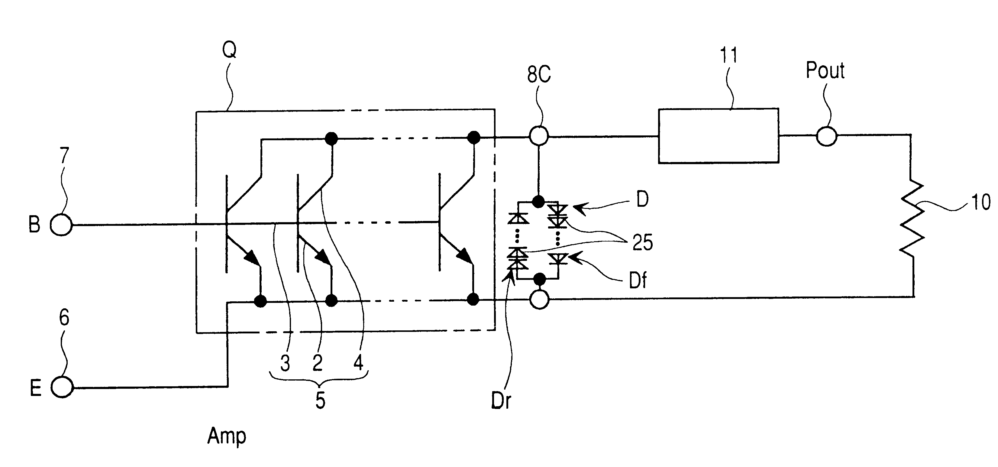
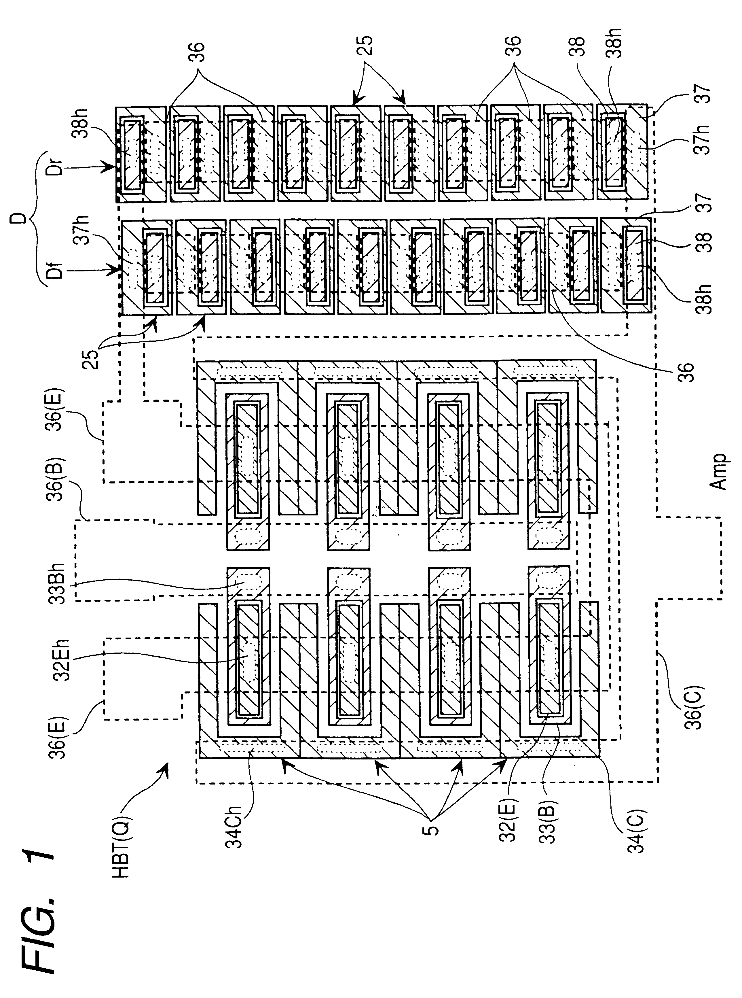
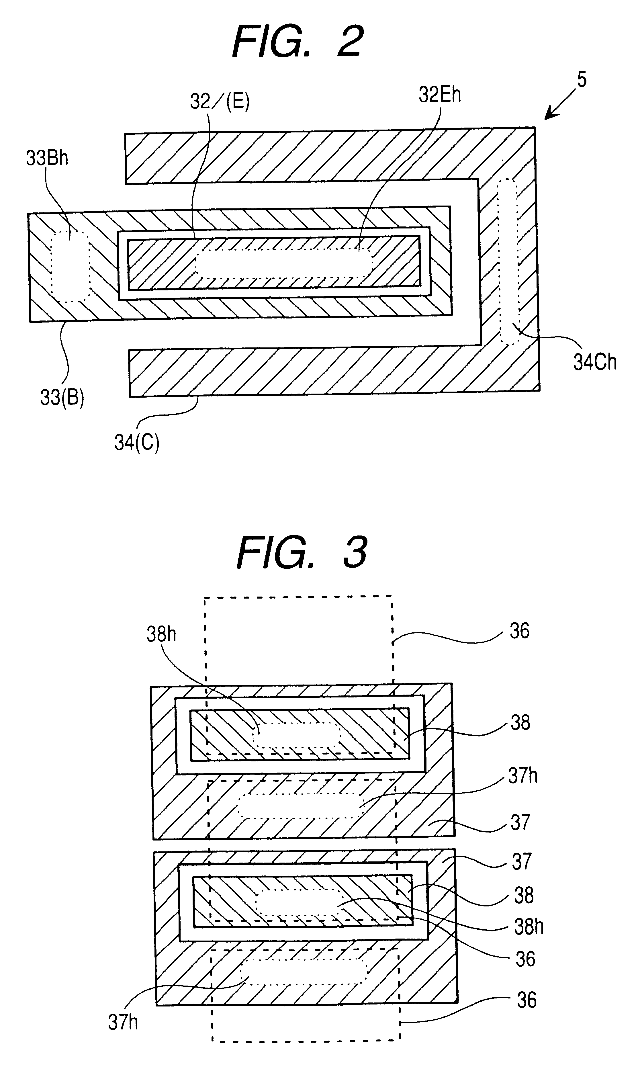
(1) In the semiconductor amplifying device with the protection circuit in the RF power amplifier module, between the first terminal (collector terminal) connected to the output terminal (Pout) and the second terminal (emitter terminal), the first protection circuit (Df) having the rectifying characteristic in the forward direction in accordance with the voltage at the collector terminal and the second protection circuit (Dr) which displays the rectifying characteristic in the reverse direction when the first protection circuit displays the rectifying characteristic in the forward direction are provided.

Each of the protection circuits has the configuration in which (n) pn junction diodes are connected in series. The (n) pn junction diodes connected in series effectively have the diode characteristic of an ON-state voltage (=n.times.V.sub.f). Consequently, even when an overvoltage is applied across the collector and the emitter, the ...

second embodiment

FIG. 17 is a schematic plan view showing a multi-finger pattern of an HBT with a protection circuit in an RF power amplifier module according to another embodiment (second embodiment) of the invention. In the second embodiment, the protection circuit (Dr) having the rectifying characteristic in the reverse direction has the pn junction diodes 25 of the number which is smaller than that in the case of the protection circuit (Df) having the rectifying characteristic in the forward direction and is set to two. This structure is created on the basis of the idea such that noise in the reverse direction is smaller than that in the forward direction. With the structure, the size of the semiconductor amplifying device (Amp) with the protection circuit can be reduced.

third embodiment

FIG. 18 is a schematic plan view showing a multi-finger pattern of an HBT with a protection circuit in an RF power amplifier module according to another embodiment (third embodiment) of the invention. In the third embodiment, the protection circuit (D) is constructed only by the protection circuit (Df) having the rectifying characteristic in the reverse direction. This configuration can be used in the case where noise in the reverse direction does not have to be considered. With the configuration, the size of the semiconductor amplifying device (Amp) with a protection circuit can be reduced.


PUM


Abstract

In a high frequency power amplifier module of a multi-stage structure in which a plurality of heterojunction bipolar transistors (npn-type HBTs) are cascade-connected, a protection circuit in which a plurality of pn junction diodes are connected in series is connected between the collector and emitter of each HBT. The p-side is connected to the collector side, and the n-side is connected to the emitter side. A protection circuit in which pn junction diodes of the number equal to or smaller than that of the pn junction diodes are connected in series is connected between the base and the emitter. The p-side is connected to the base side, and the n-side is connected to the emitter side. With the configuration, in the case where an overvoltage is applied across the collector and emitter due to a fluctuation in load on the antenna side, the collector terminal is clamped by an ON-state voltage of the protection circuits, so that the HBT can be prevented from being destroyed. Since the similar protection circuit is assembled between the base and emitter, even when the operator touches the module at the time of manufacturing the high frequency power amplifier module, the HBT can be prevented from being destroyed by the clamping effect of the protection circuit between the base and emitter and the protection circuit between the collector and emitter. Thus, an improved manufacturing yield of the high frequency power amplifier module and a wireless communication apparatus can be achieved, and destruction caused by fluctuation in load impedance of the wireless communication apparatus can be prevented.

Description

The present invention relates to a high frequency power amplifier module for obtaining a predetermined amplification factor by cascade connecting a plurality of heterojunction bipolar transistors, and a wireless communication apparatus in which the high frequency power amplifier module is assembled. More particularly, the invention relates to a technique effective for improving destruction resistance of a heterojunction bipolar transistor to fluctuations in load impedance.At an input stage of a transmitter of a wireless communication apparatus (mobile communication apparatus) such as an automobile telephone or portable telephone, an amplifier (high frequency power amplifier module, or RF power module) in which MOSFETs (Metal Oxide Semiconductor Field-Effect-Transistors), GaAs-MES (Metal-Semiconductor) FETs, HEMTs (High Electron Mobility Transistors), or HBTs (Heterojunction Bipolar Transistors) are formed at multiple stages is assembled.The heterojunction bipolar transistor (HBT) is...

Claims


Application Information

Patent Timeline
IPC IPC(8): H01L27/02H03F3/189H03F1/52H03F3/195
CPCH01L27/0255H03F1/52H03F3/195H03F2203/21178H03F2200/444
Inventor KUSANO, CYUSHIROHASE, EIICHIONO, HIDEYUKIKAGAYA, OSAMUUMEMOTO, YASUNARIFUJITA, TAKAHIROYAMASHITA, KIICHI
Owner RENESAS ELECTRONICS CORP
Why Eureka
Try Eureka