

Method of reading stored data and semiconductor memory device
a technology of memory device and stored data, which is applied in the direction of semiconductor devices, digital storage, instruments, etc., can solve the problems of degrading the quality of memory, increasing the number of elements, and falling the degree of integration
- Summary
- Abstract
- Description
- Claims
- Application Information
AI Technical Summary
Benefits of technology
Problems solved by technology
Method used
Image

Examples
first embodiment
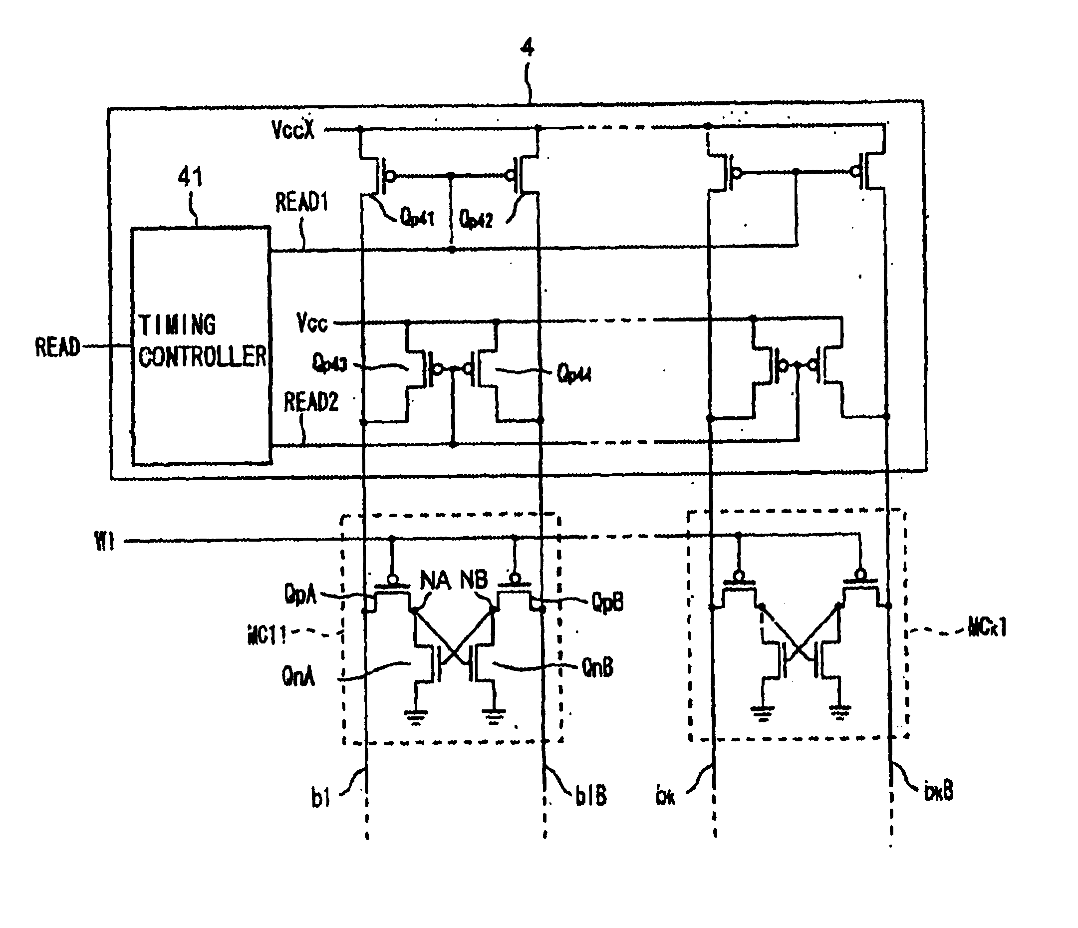
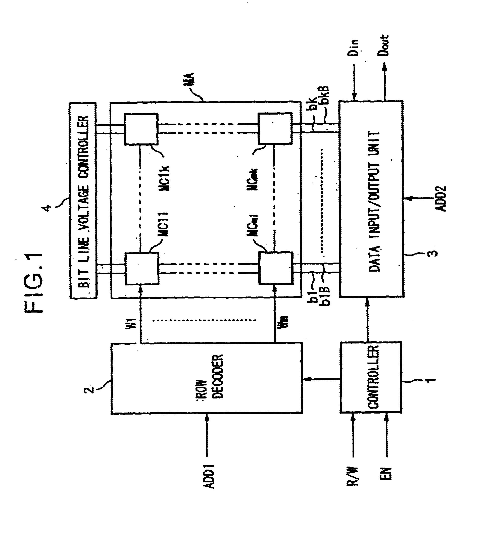
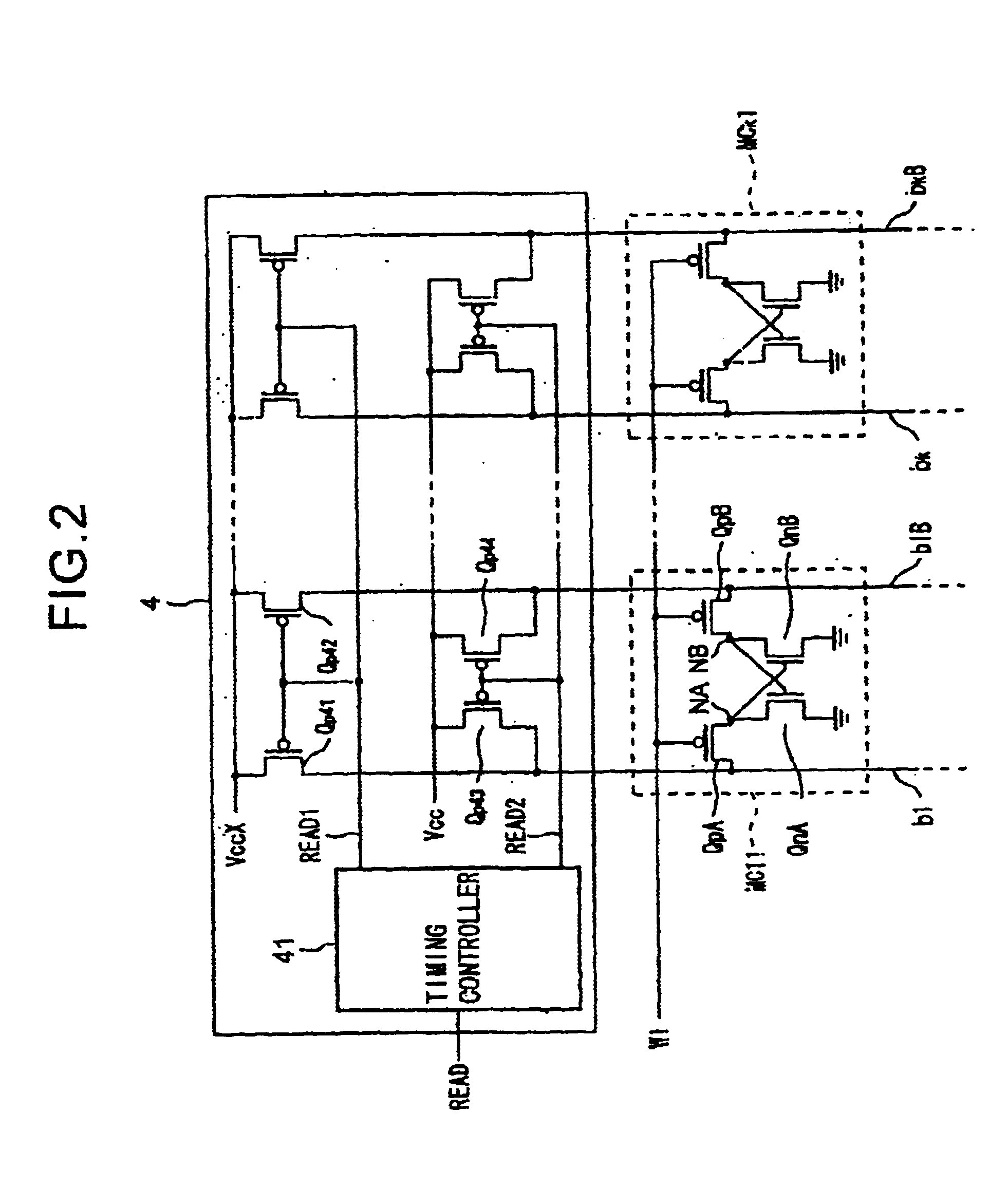
FIG. 1 is a schematic view of an example of the configuration of a SRAM according to the present invention. The SRAM shown in FIG. 1 includes a controller 1, row decoder 2, data input / output unit 3, bit line voltage controller 4, and memory cell array MA. Also, the memory cell array MA includes a memory cell MC11 to memory cell MCmk.
When an enable signal EN is set to an active state, the controller 1 outputs various control signals for the read or write operation of data selected in accordance with a selection signal R / W to the row decoder 2, data input / output unit 3, and bit line voltage controller 4 to control the write or read operation of the data with respect to the memory cell array MA.
The row decoder 2 decodes address data ADD1 in accordance with the control signal from the controller 1 at the time of reading or writing of the data and selects and activates one of a word line W1 to word line Wm connected to the memory cell MC11 to the memory cell MCmk of the memory cell array...
second embodiment
Next, an explanation will be made of a second embodiment of the present invention.
FIG. 8 is a schematic block diagram of an example of the configuration of an associative memory according to the second embodiment of the present invention.
The associative memory shown in FIG. 8 has an address controller 11, CAM cell array 12, data input / output unit 13, search result register 14, priority encoder 15, address power supply unit 16, and data power supply unit 17.
The address controller 11 receives an address data EX_ADD input from the outside or an address data M_ADD of the search result selected at the priority encoder, selects the word line of the CAM cell array 12 corresponding to the input address data, and activates the selected word line at the time of writing and the time of reading of the data. In the period for holding the stored data and at the time of the match search explained later, all word lines are deactivated, and access from the bit lines to the CAM cells is prohibited.
Th...
third embodiment
Next, an explanation will be made of a third embodiment of the present invention. The difference between the second embodiment and the third embodiment resides in the point that the configuration of the logical circuit portion for outputting the match search result to the mismatch detection line ML in the CAM cell is different.
Note that, the overall configuration of the associative memory is similar to that of FIG. 8, so the explanation is omitted, and just the binary CAM cell will be explained by referring to FIG. 11.
FIG. 11 is a circuit diagram showing the example of the configuration of the binary CAM cell according to the third embodiment of the present invention.
In FIG. 11, notation Qp203 and notation Qp204 designate p-type MOS transistors, notation Qn201, notation Qn202, and notation Qn205 to notation Qn207 designate n-type MOS transistors, notation WL designates the word line, notation BL and notation / BL designate the bit line pair, and notation ML designates the mismatch det...
PUM
 Abstract
Description
Claims
Application Information