Ceramic electronic device and method of production of same

a ceramic electronic device and ceramic coating technology, applied in the manufacture of fixed capacitors, fixed capacitor details, fixed capacitors, etc., can solve the problems of difficult peeling off of ceramic coating layers from the substrate, no longer able to obtain targeted electrostatic capacity, and holes or wrinkles in ceramic coating layers

Inactive Publication Date: 2004-08-24
TDK CORPARATION
View PDF19 Cites 14 Cited by
  • Summary
  • Abstract
  • Description
  • Claims
  • Application Information

AI Technical Summary

Benefits of technology

Another object of the present invention is to provide a method of production of a high precision, high reliability ceramic electronic device able to remarkably reduce the difficulty in peeling and probability of occurrence of defects in characteristics of the product even if reducing the thickness of the ceramic coating layers.
Preferably, there is at least one ceramic layer configured by a second ceramic layer alone between pairs of adjoining ceramic layers of multilayer structures comprised of the first ceramic layer and third ceramic layer. In this case, it is possible to increase the total thickness in each stacked unit (stacked group) and reduce the times of stacking the stacked units,

Problems solved by technology

When printing an internal electrode paste of such a composition on a ceramic coating layer coated on a substrate in accordance with the conventional method of production, however, the terpineol, methyl ethyl ketone, or other organic solvent contained in the internal electrode paste ends up dissolving the acrylic resin, butyral resin, or other organic binder contained in the ceramic coating layer.
If sheet attack occurs, it becomes difficult to peel off the ceramic coating layer from the substrate.
Further, sometimes holes or wrinkles occur in the ceramic coating layer.
If using such a ceramic coating layer to produce a multilayer ceramic capacitor, short-circuit defects where internal electrodes become connected will arise, withstand voltage defects will arise, the targeted electrostatic capacity will no longer be able to be obtained, or other critical defects are liable to occur.
With this method, however, the adhesion of the internal electrode and ceramic coating layer with respect to the substrate becomes stronger, so it becomes extremely difficult to peel off the ceramic coating layer without damage (holes, wrinkles, tears, etc.)
When printing an internal electrode on the surface of a peeling agent, however, since the affinity between the two is low, the internal electrode is subjected to an agglomerating action due to the surface tension, the shape of the pattern of internal electrode ends up being ruined, and the desired characteristics can no longer be obtained.
If the thickness T1 of the first ceramic coating layer becomes 1.5 .mu.m or more, the short-circuit defect rate will be lowered, but there will be a tendency for the withstand voltage defect rate to become higher.
If the thickness T1 of the first ceramic layer becomes 1.5 .mu.m or more, the short-circuit defect rate will be lowered, but there is a tendency for the withstand voltage defect rate to become higher.
If the mean particle size .alpha.1 becomes smaller than 0.05 .mu.m, there will be a tendency for the dispersibility of the ceramic particles at the time of preparing the ceramic coating to deteriorate and for formation of a uniform ceramic coating layer to become impossible.
If the mean particle size .alpha.1 of the ceramic particles exceeds 0.35 .mu.m, there will be a tendency for short-circuit defects and withstand voltage defects to occur easily.
Further, the short-circuit defect rate was found by applying a 2 V DC voltage, judging the insulation resistance under 1.times.10 a as being defective, and finding the percentage of the number of defects.

Method used


Image

  • Ceramic electronic device and method of production of same
  • Ceramic electronic device and method of production of same
  • Ceramic electronic device and method of production of same

Examples


second embodiment

Next, a multilayer ceramic capacitor according to another embodiment of the present invention will be explained.

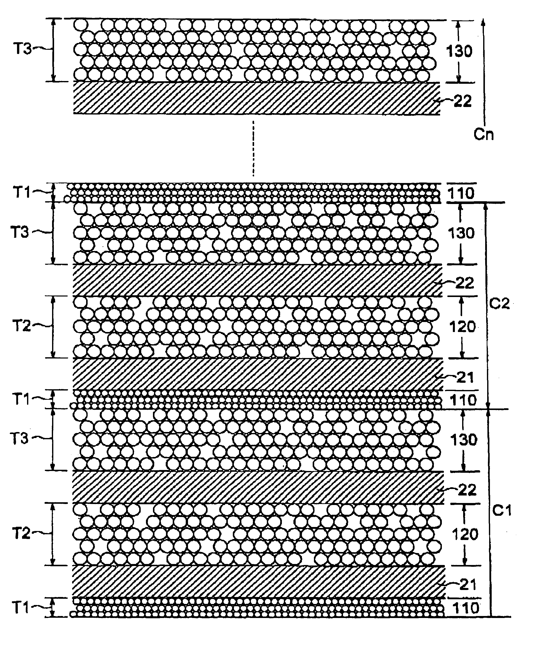
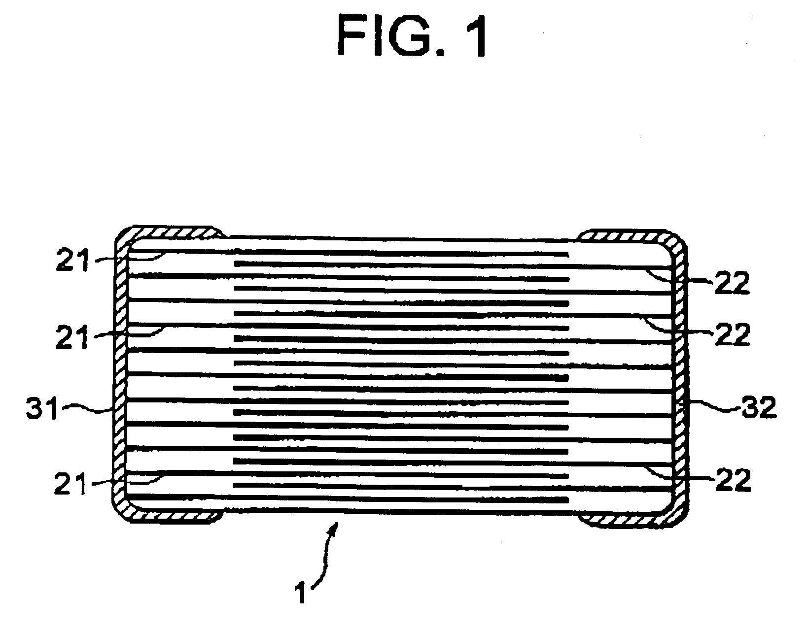
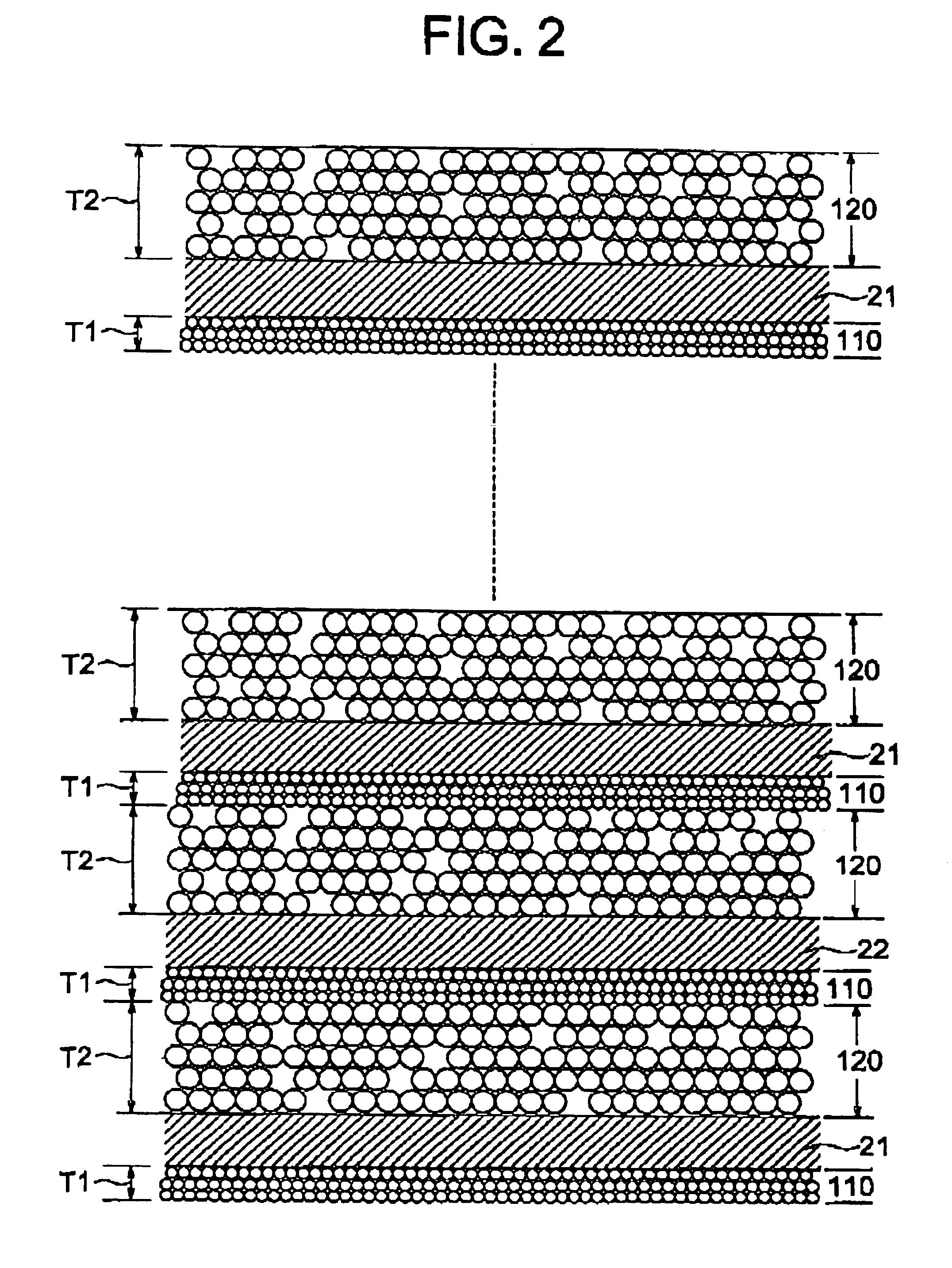
FIG. 15 is an enlarged cross-sectional view schematically showing the internal structure of a multilayer ceramic capacitor according to a second embodiment of the present invention. For convenience in illustration, the middle part is not shown. The overall cross-section of the multilayer ceramic capacitor according to the present embodiment is the same as that shown in FIG. 1 and includes the ceramic body 1, internal electrodes 21 and 22, and terminal electrodes 31 and 32. In the present embodiment, however, as shown in FIG. 15, the ceramic body 1 includes first ceramic layers 110, second ceramic layers 120, and third ceramic layers 130. Note that at least one ceramic layer present between pairs of adjoining internal electrodes 21 and 22 is a multilayer structure. From this viewpoint, the third ceramic layer 130 in the present embodiment corresponds to the second ceramic l...


PUM

PropertyMeasurementUnit
thicknessaaaaaaaaaa
thicknessaaaaaaaaaa
thicknessesaaaaaaaaaa

Abstract

A method of production of a ceramic electronic device such as a multilayer ceramic capacitor, comprising forming a first ceramic coating layer on the surface of a substrate, forming an internal electrode on the surface of the first ceramic coating layer, then forming a second ceramic coating layer on the surface of the first ceramic coating layer so as to cover the internal electrode. In this case, when a mean particle size of ceramic particles of the first ceramic coating layer is alpha1, a thickness of the first ceramic coating layer is T1, a mean particle size of ceramic particles of the second ceramic coating layer is alpha2, and a thickness of the second ceramic coating layer is T2, the conditions of alpha1<=alpha2, 0.05<alpha1<=0.35 mum, T1<T2, and 0<T1<1.5 mum are satisfied. As a result, it is possible to provide a ceramic electronic device, in particular a multilayer ceramic capacitor, resistant to short-circuit defects, withstand voltage defects, and other structural defects.

Description

1. Field of the InventionThe present invention relates to a ceramic electronic device and a method of production of the same.2. Description of the Related ArtAs one method for producing a capacitor, piezoelectric device, or other ceramic electronic device, there is known the method of forming a ceramic coating in a sheet on a substrate by the doctor blade method to obtain a green sheet and forming electrode paste on top of this by screen printing. In this case, the ceramic coating includes ceramic powder, an organic binder, a plasticizer, a solvent, etc., while the electrode paste includes palladium, silver, nickel, or other conductive particles.When desiring to obtain a multilayer structure, green sheets formed with the electrode paste layers are stacked to the desired multilayer structure and then cut by a press to obtain ceramic green chips. The thus obtained ceramic green chips are processed to remove the binder, then fired at 1000.degree. C. to 1400.degree. C. Silver, silver-pa...

Claims


Application Information

Patent Timeline
Patent Type & Authority Patents(United States)
IPC IPC(8): B32B3/00B32B9/00H01G4/30H01G4/20H01G4/12H01G4/018H01G4/06H01G13/00H01L41/24H05H1/02H05K3/36
CPCH01G4/30Y10T29/49126Y10T29/49117Y10T29/49128Y10T428/24975Y10T428/24917Y10T428/252Y10T428/24926Y10T29/435Y10T29/49155
Inventor KOBAYASHI, RYOUUEDA, KANAMEIZUMIBE, YASUSHIISHIDA, HITOSHISAITOH, AKIRA
Owner TDK CORPARATION
Why Eureka
Try Eureka