Substrate processing apparatus, substrate inspection method and substrate processing system
- Summary
- Abstract
- Description
- Claims
- Application Information
AI Technical Summary
Benefits of technology
Problems solved by technology
Method used
Image

Examples
Embodiment Construction
An embodiment of the present invention is now described in detail with reference to the drawings.
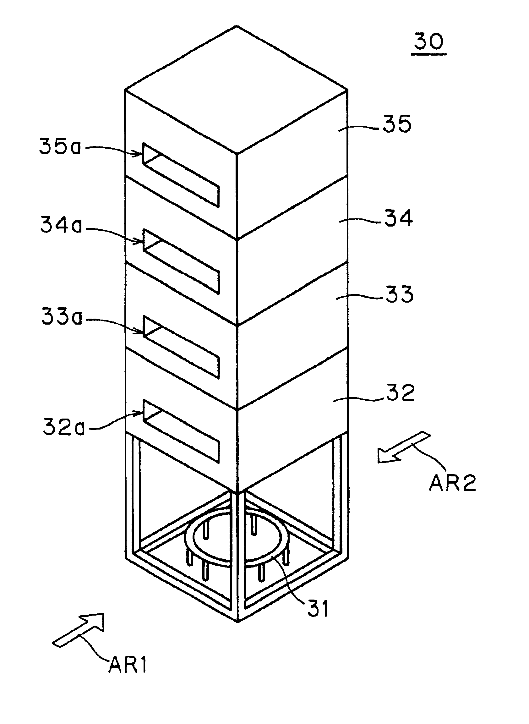
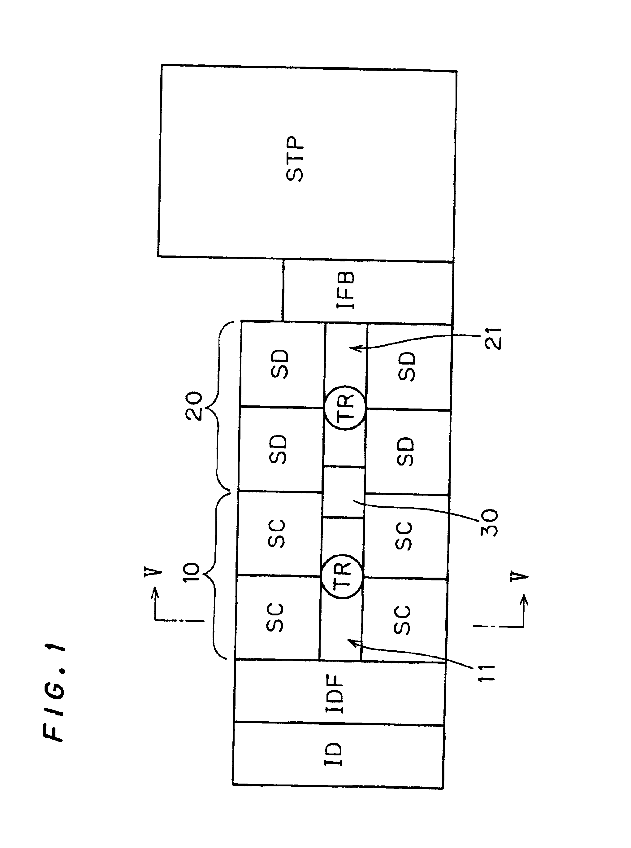
FIG. 1 is a plan view showing the arrangement / structure of a substrate processing apparatus according to the present invention. This substrate processing apparatus, performing photoresist coating processing and development processing on a substrate, comprises coating units 10 performing resist coating processing, development units 20 performing development processing, an indexer ID introducing the substrate into the processing units 10 and 20, an indexer transfer part IDF and an interface IFB. In the substrate processing apparatus, an inspection unit 30 is arranged between the coating units 10 and the development units 20. Further, an exposure unit STP (the so-called stepper) performing exposure processing is arranged outside the substrate processing apparatus, in contact with the interface IFB.
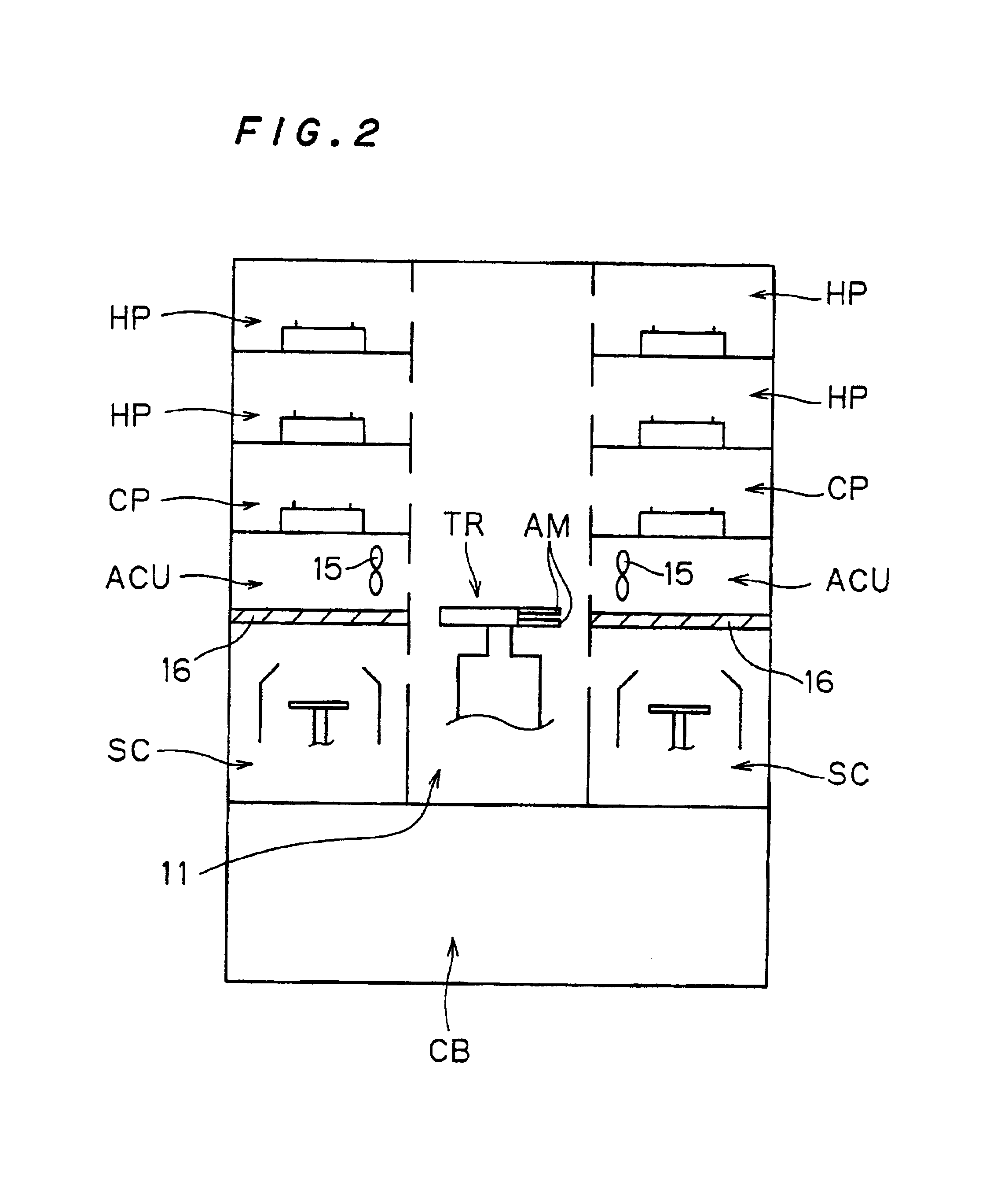
Two pairs of coating parts SC are provided in the coating units 10 through a transport path 11...
PUM
| Property | Measurement | Unit |
|---|---|---|
| Thickness | aaaaa | aaaaa |
| Content | aaaaa | aaaaa |
| Transport properties | aaaaa | aaaaa |
Abstract
Description
Claims
Application Information
 - Generate Ideas
- Intellectual Property
- Life Sciences
- Materials
- Tech Scout
- Unparalleled Data Quality
- Higher Quality Content
- 60% Fewer Hallucinations
Browse by: Latest US Patents, China's latest patents, Technical Efficacy Thesaurus, Application Domain, Technology Topic, Popular Technical Reports.
© 2025 PatSnap. All rights reserved.Legal|Privacy policy|Modern Slavery Act Transparency Statement|Sitemap|About US| Contact US: help@patsnap.com