Concurrent logical and physical construction of voltage islands for mixed supply voltage designs

a technology of voltage islands and circuits, applied in the field of computer-aided placement of circuits, can solve the problems of reducing circuit performance, islands may not be conducive to good logical placement, and reducing circuit performance, so as to reduce power distribution costs, reduce the number of level shifters used, and improve logical placement

Inactive Publication Date: 2004-09-14
IBM CORP
View PDF16 Cites 64 Cited by
  • Summary
  • Abstract
  • Description
  • Claims
  • Application Information

AI Technical Summary

Benefits of technology

, placing high voltage circuits in high voltage islands and low voltage circuits in low voltage islands typically minimizes the number of level shifters used. This also reduces the number of places to which the high and low voltage power must route, thereby reducing power distribution costs. However, these islands may not be conducive to good logical placement. For example, a signal might have to run quite a long distance to a high voltage island and then from the high voltage island back to circuitry that uses this signal. This could actually decrease performance instead of increasing it. Thus, a poor placement result occurs for what should be a better placement.
Another method used for creating high and low voltage circuits is logical clustering. In logical cluster, the high and low voltage circuits are designed--not in voltage islands--based on connectivity. Elements in a circuit that need to be faster are changed to higher voltage, while slower, non-critical elements are changed to lower voltage. This solves the placement issues caused by high and low voltage island clustering, as the data paths are not moved. However, the different power supplies must be distributed everywhere and logical clustering can tremendously increase the number of level shifters.
The preferred embodiments of the present invention solve these problems by providing both logical and physical construction of voltage islands. The preferred embodiments of the present invention combine both physical and logical synthesis to provide fewer level shifters and less power routing, but still meet timing and other requirements. Additionally, by using an iterative process for construction of the voltage islands, power usage can be minimized while speed constraints, in particular, are met.
In one aspect of the present invention, a semiconductor chip design is partitioned into "bins", which are areas of the design. In this way, a semiconductor chip design may be "sliced" into various areas and the areas may then be assigned to various voltage levels. Each bin may be thought of as a voltage island. Circuits in the design can be added to or removed from the various bins, thereby increasing or decreasing the speed and power of the circuits: the speed and power increase if a circuit is placed into a bin assigned a higher voltage, and the speed and power decrease if a circuit is placed into a bin having a lower voltage. The size and location of the bins may also be changed. By iterating these steps, the optimum power consumption may be met while still meeting speed constraints and other criteria.

Problems solved by technology

However, reduction in power supply voltage also reduces circuit performance.
However, these islands may not be conducive to good logical placement.
This could actually decrease performance instead of increasing it.
Thus, a poor placement result occurs for what should be a better placement.
However, the different power supplies must be distributed everywhere and logical clustering can tremendously increase the number of level shifters.

Method used


Image

  • Concurrent logical and physical construction of voltage islands for mixed supply voltage designs
  • Concurrent logical and physical construction of voltage islands for mixed supply voltage designs
  • Concurrent logical and physical construction of voltage islands for mixed supply voltage designs

Examples


Embodiment Construction

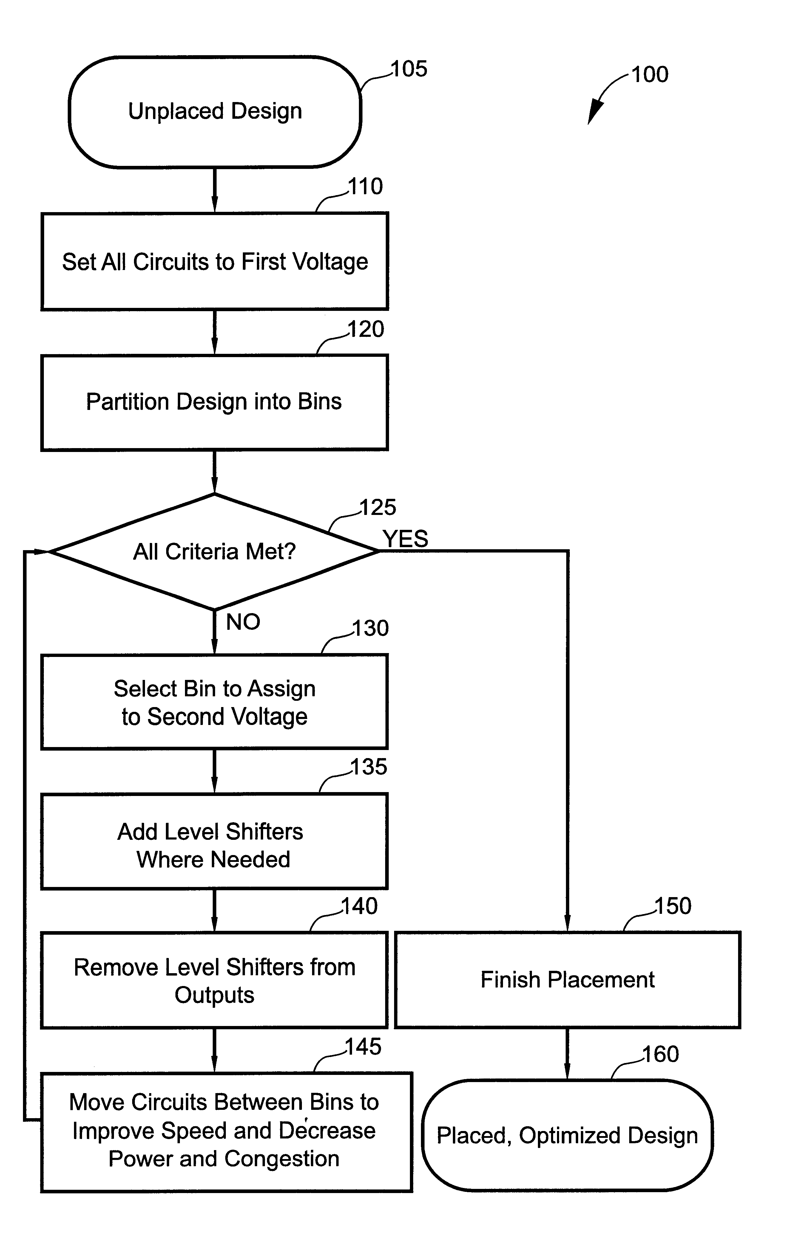
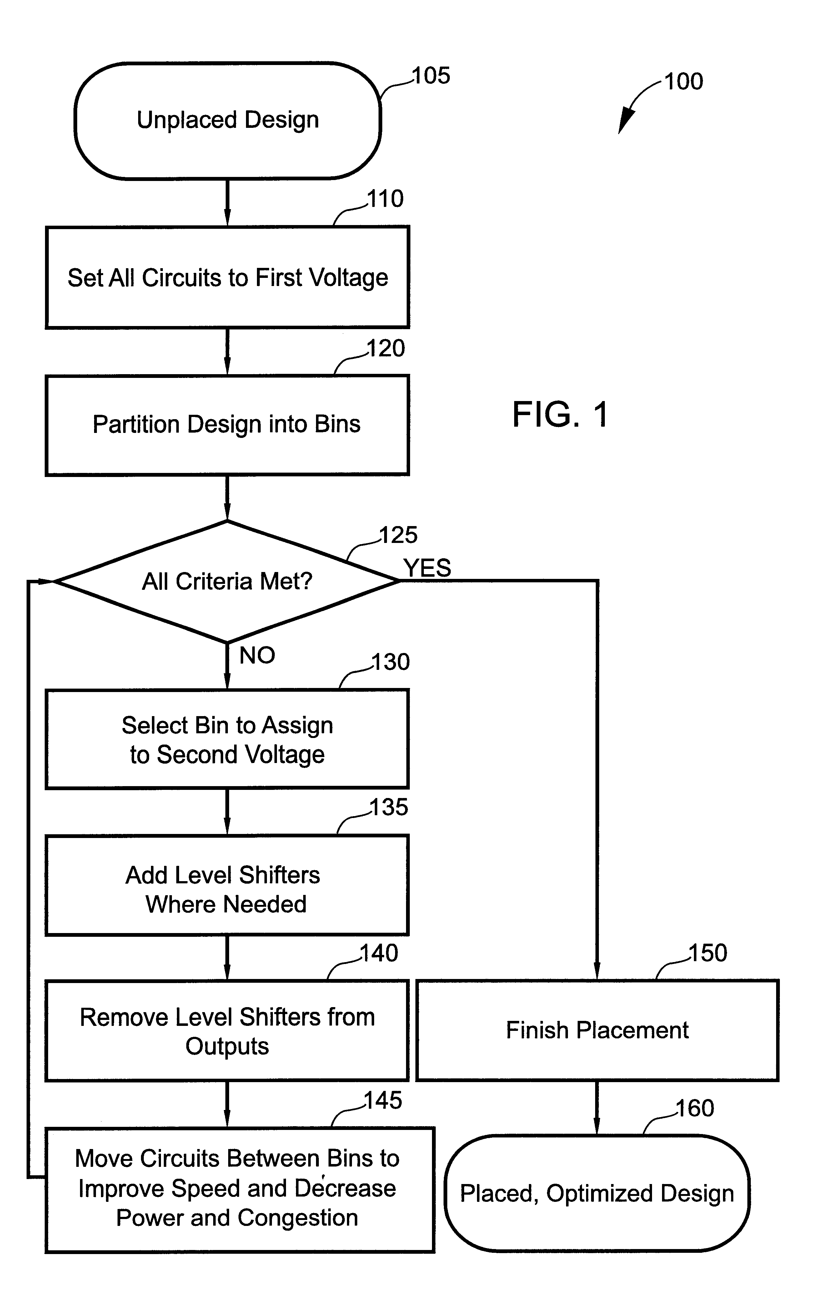
As stated previously, the present invention relates to computer-aided placement of circuits on a semiconductor chip. For those not familiar with this topic, the following Overview section briefly introduces some of the concepts associated with placement processes. Those skilled in the art of computer-aided placement of circuits on a semiconductor chip may wish to proceed directly to the Detailed Description.

Overview

When a semiconductor chip is designed, computer design tools are used. These tools work on and produce a file called a "netlist." This netlist contains a description of all of the gates and the connections between them. A semiconductor chip designer generally works with a simulated logical layout of the chip. In other words, the semiconductor chip will perform some function, and the designer ensures that the simulated chip actually logically performs the function. When the actual chip is ready to be made, chip designers use a placement tool that takes the original netlist...


PUM


Abstract

Both logical and physical construction of voltage islands is disclosed. A semiconductor chip design is partitioned into "bins", which are areas of the design. In this way, a semiconductor chip design may be "sliced" into various areas and the areas may then be assigned to various voltage levels. Each bin may be thought of as a voltage island. Circuits in the design can be added to or removed from the various bins, thereby increasing or decreasing the speed and power of the circuits: the speed and power increase if a circuit is placed into a bin assigned a higher voltage, and the speed and power decrease if a circuit is placed into a bin having a lower voltage. The size and location of the bins may also be changed. By iterating these steps, the optimum power consumption may be met while still meeting speed constraints and other criteria. The present invention is applicable to any placement environment, such as an annealing placement tool, that proceeds through successive refinement of the locations of the circuits on the design and in which the placement process may be interrupted to make changes in placement of the logic.

Description

1. Technical FieldThis invention generally relates to computer-aided placement of circuits on a semiconductor chip, and more specifically relates to concurrent logical and physical construction of voltage islands for mixed supply voltage designs.2. Background ArtThe switching power of digital circuits increases as the square of the power supply voltage increases. Thus, reducing this voltage is desirable for reduction in circuit power consumption. However, reduction in power supply voltage also reduces circuit performance. Therefore, it is desirable to combine circuits driven by a higher power supply voltage and circuits driven by a lower power supply voltage (hereafter referred to as high and low voltage circuits, respectively) on the same chip. The high voltage circuits are used where needed to achieve the desired circuit performance and the low voltage circuits are used elsewhere.When high and low voltage circuits are combined on a semiconductor chip in this way, it is desirable t...

Claims


Application Information

Patent Timeline
Patent Type & Authority Patents(United States)
IPC IPC(8): G06F17/50H01L21/82
CPCG06F17/5045G06F17/5068G06F30/39G06F30/30
Inventor COHN, JOHN MDEAN, ALVAR A.HATHAWAY, DAVID J.LACKEY, DAVID E.LEPSIC, THOMAS M.LICHTENSTEIGER, SUSAN K.TETREAULT, SCOTT A.VENTRONE, SEBASTIAN T.
Owner IBM CORP
Why Eureka
Try Eureka