Use of a free space electron switch in a telecommunications network

a free space electron switch and telecommunications network technology, applied in the field of electron switch, can solve the problems of reducing the optical signal strength, reducing the detection efficiency of optical signals over background noise, and requiring the receiver to provide suitable photon switching devices to redirect optical signals,

Inactive Publication Date: 2004-10-05
EXACONNECT
View PDF72 Cites 49 Cited by
  • Summary
  • Abstract
  • Description
  • Claims
  • Application Information

AI Technical Summary

Problems solved by technology

When optical signals are transmitted over great distances through optical fibers, attenuation within the fibers reduces the optical signal strength.
Therefore, detection of the optical signals over background noise becomes more difficult at the receiver.
Because photons are highly non-reactive to the propagation medium of the optical fiber and to each other, providing suitable photon switching devices to redirect the optical signal is typically difficult.
Further, pure optical switching is difficult to achieve because photons cannot be directed or steered without modifying the physical medium through which they propagate.
Because the process of modifying the physical medium to steer an optical beam tends to be slow and unwieldy, few photon switching technologies provide a fast enough response time necessary for state-of-the-art optical switching speeds, and those that may be fast enough typically cannot be scaled suitably to provide a sufficient number of output ports.
Digital MEMS switches potentially provide a relatively low switching speed (latency), but are not scaleable.
Further, the number of internal components in a digital MEMS switch increases exponentially as the number of output ports increases, making them difficult to scale beyond a few hundred ports.
However, analog MEMS switches typically have a high switching latency (low switching speed) requiring milliseconds to switch.
The longevity and reliability of MEMS switches for optical signal switching applications are suspect.
Therefore, if an analog MEM switch could operate fast enough to switch optical packets at commercially acceptable speeds, the switch would barely survive one minute before reaching the end of its operating life.
Further, MEMS switches are sensitive to shocks, are fragile, and are bulky.
Additionally, current generation MEMS switches require the use of regenerator lasers, even in course, fiber-by-fiber switching applications, because of the lack of reflectivity of the mirrors.
However, it is not clear that this will eliminate the need for regenerator lasers, especially in real-world networks that have multiple hops and long-transmission lengths.
Tunable lasers do not mitigate this problem, because they still require that a given wavelength signal be reserved from end-to-end of the network.
However, all of these technologies typically suffer from lack of scalability and have a high switching latency.
Also, the de-multiplexers and multiplexers that separate the bit stream and then recombine the stream is complex and requires exotic switching technology, especially for OC-192 bit rates and beyond.
As a result, CLOS interconnected crossbar switches have very large footprints, and consume a large amount of power.
Switching speed has also presented a problem with CLOS-based switches.
Moreover, their switching speed is non-deterministic, in that the amount of time needed to establish a connection is highly unpredictable.
For packet-by-packet switching applications, the complexity of the packet forwarding engines and traffic managers that control the switch is greatly increased because it is difficult for the switch to guarantee FIFO packet behavior.
Further, unwanted effects are introduced into the output packet stream, such as jitter.
It is likely that many of the CLOS crossbar-based electronic switches that are used within OEO optical cross-connects have such a slow switching speed and are highly unpredictable that they may not be suitable for packet-by-packet switching.
Board-to-board connector density is also a serious concern with CLOS switches.
Therefore, CLOS based switches are limited by the connector density, trace density and interconnects needed to create all of the internal intra-switch bandwidth.
As a result, it has been suggested that CLOS switches hit hard limits in terms of board-to-board connector density at 512 output ports.
Also, as with all semiconductor logic-based switches, bit rate per port is limited by the clock rate of the logic gates.
Thus, as discussed above, these devices have proved complex and difficult to scale for switching applications, and they are limited by the speed at which their solid-state logic gates are capable of switching.

Method used


Image

  • Use of a free space electron switch in a telecommunications network
  • Use of a free space electron switch in a telecommunications network
  • Use of a free space electron switch in a telecommunications network

Examples


Embodiment Construction

The following discussion of the embodiments of the invention directed to a free space electron switch used in conjunction with various telecommunication systems is merely exemplary in nature, and is in no way intended to limit the invention or its applications or uses.

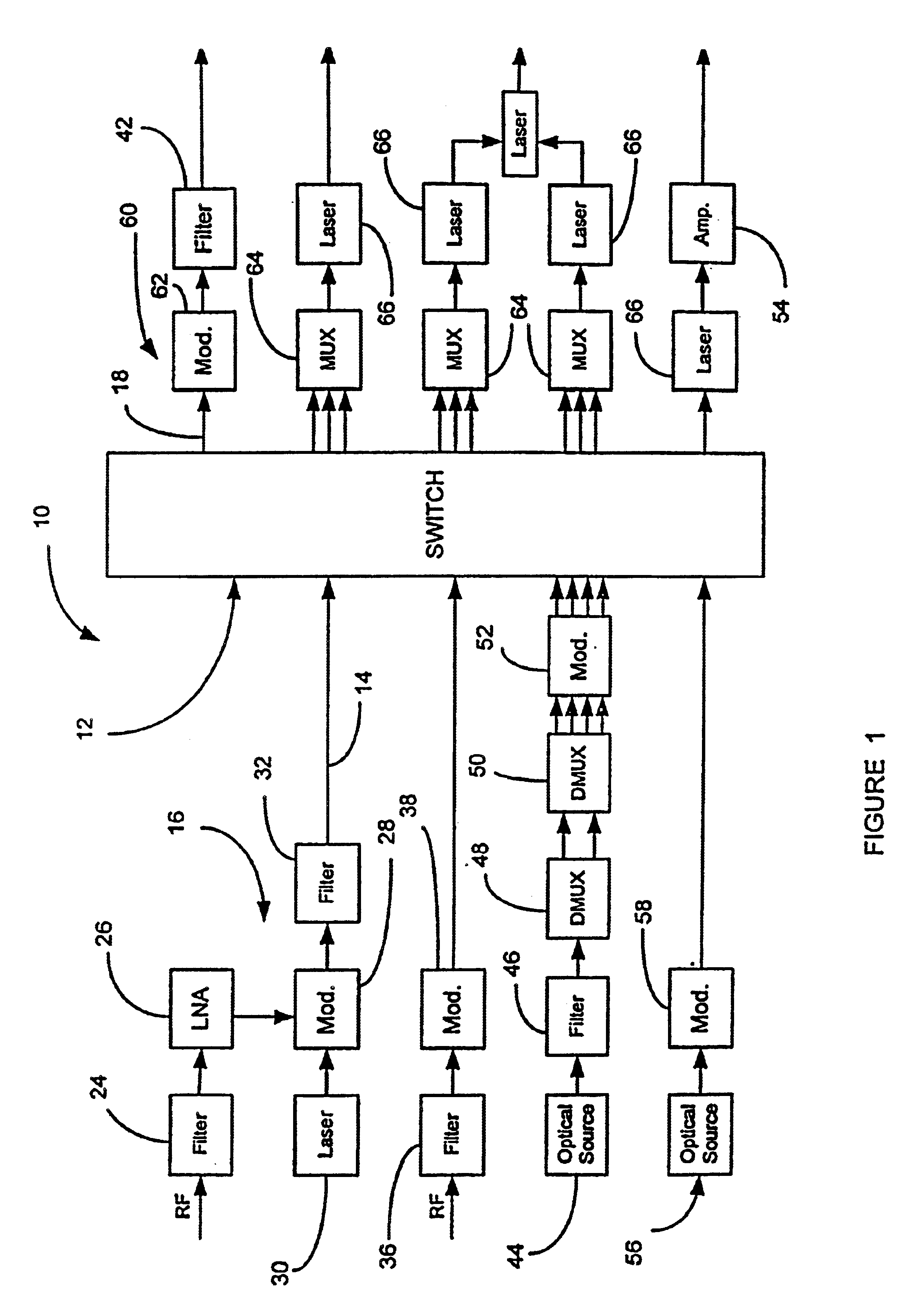
FIG. 1 is a block diagram of a telecommunications system 10 employing a free space electron switch 12, according to the invention. The switch 12 is responsive to a plurality of optical signals and RF signals on input lines 14 in connection with various communications channels 16. Only a few of the channels are shown, but, as would be appreciated by those skilled in the art, a practical switch of the type discussed herein would have thousands of input channels. As will be discussed in detail below, the switch 12 directs or switches the signals on the various input lines 14 to one or more of a plurality of output lines 18 in connection with various communications channels 20 at the output of the switch 12. The electron s...


PUM


Abstract

A communications system that includes one or more free space electron switches. The free space electron switch employs an array of electron emitters, where each emitter is responsive to an RF or optical input signal on an input channel. Each emitter includes a cathode that emits electrons in response to the input signal. Each emitter further includes a focussing / accelerating electrode for collecting and accelerating the emitted electrons into an electron beam. Each emitter further includes an aiming anode that directs the beam of electrons to a desired detector within an array of detectors that converts the beam of electrons to a representative RF or optical signal on an output channel. Each emitter may include a modulating electrode that generates an electric field to modulate data onto the beam of electrons. The communications systems employing the switch can be an ISDN, DSLAM networks, packet routing systems, ADSL networks, PBX systems, local exchange systems, etc.

Description

1. Field of the InventionThis invention relates generally to an electron switch for use in a communications network and, more particularly, to a free space electron switch for switching purposes in a communications network, where the switch employs an array of cathodes, each cathode being responsive to an optical or RF input signal on a communications channel and generating free space electrons in response thereto, and where the electron beams are selectively steerable by an aiming anode towards a particular receiver in an array of receivers associated with a plurality of output channels.2. Discussion of the Related ArtState of the art telecommunications systems and networks typically employ optical fibers to transmit optical signals separated into optical packets carrying information over great distances. An optical fiber is an optical waveguide including a core having one index of refraction surrounded by a cladding having, another, lower, index of refraction so that optical signa...

Claims


Application Information

Patent Timeline
Patent Type & Authority Patents(United States)
IPC IPC(8): H01J31/00H01J31/06
CPCH01J31/06
Inventor VICTOR, MICHEL N.SILZARS, ARISMANSOUR, GERALD G.
Owner EXACONNECT
Why Eureka
Try Eureka