Synchronized write data on a high speed memory bus

a write data and high-speed memory technology, applied in the direction of memory adressing/allocation/relocation, instruments, generating/distributing signals, etc., can solve the problem that the synchronous semiconductor memory device cannot accurately determine the proper cycle of the write clock wclk, and the command and write clocks may not be synchronized

Inactive Publication Date: 2004-10-19
ROUND ROCK RES LLC
View PDF13 Cites 62 Cited by
  • Summary
  • Abstract
  • Description
  • Claims
  • Application Information

AI Technical Summary

Problems solved by technology

However, the command and write clocks may not be synchronized.
Since the phase shift is induced by a device external to a synchronous semiconductor memory device, it i

Method used


Image

  • Synchronized write data on a high speed memory bus
  • Synchronized write data on a high speed memory bus
  • Synchronized write data on a high speed memory bus

Examples


Embodiment Construction

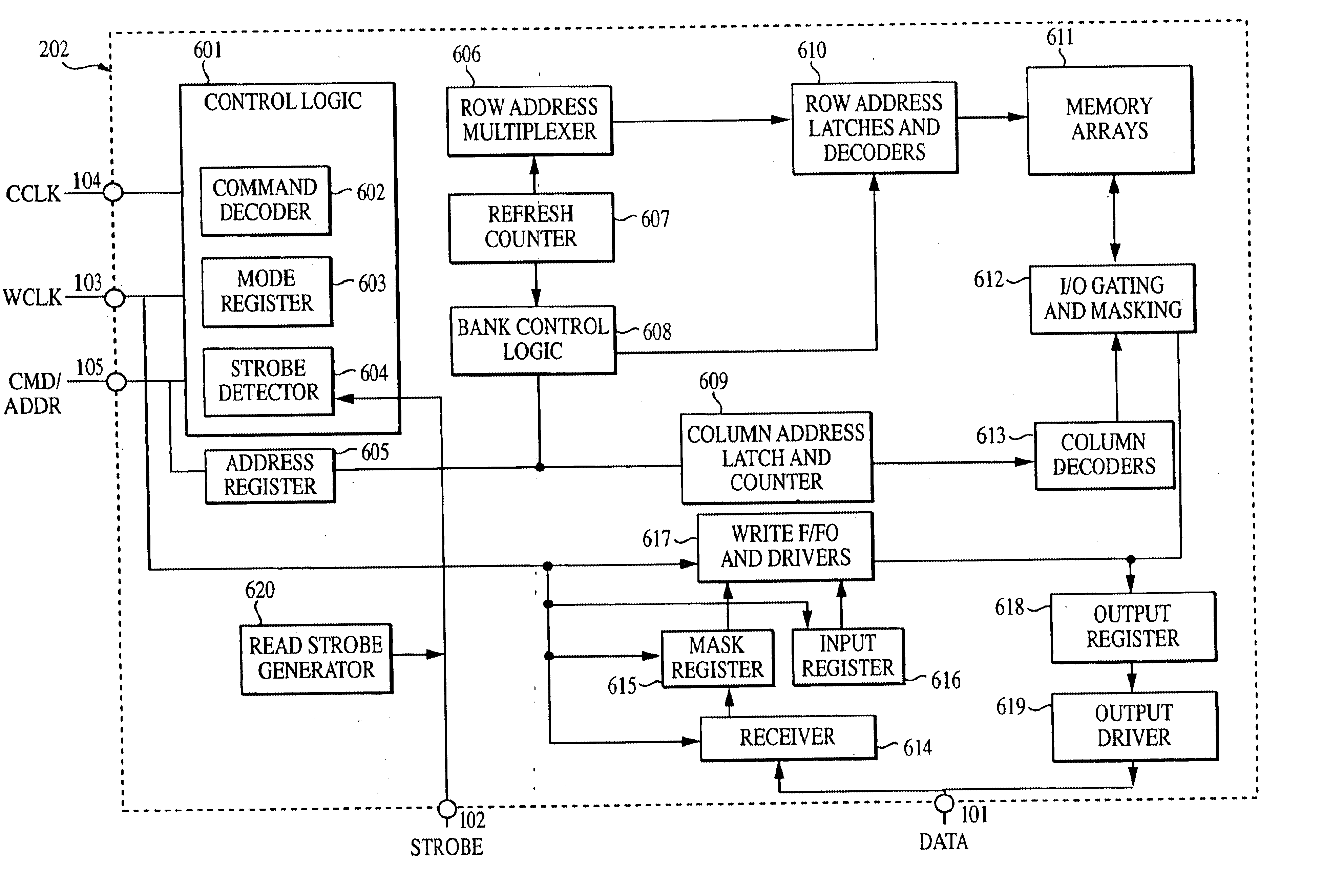
Now referring to the drawings, where like reference numerals designate like elements, there is shown in FIG. 3 a more detailed diagram of one synchronous semiconductor memory device, e.g., device 202 of FIG. 2. In the exemplary embodiment, the synchronous semiconductor memory device is a double data rate SDRAM with independent command and write clocks. A double data rate SDRAM is an SDRAM which accepts write data on both the rising and falling transitions of the write clock. Each rising or falling transition of the write clock cycle is known as a tick. The synchronous semiconductor memory device includes a variety of circuits used to control, address, and input / output data. For example, the synchronous semiconductor memory device includes a control logic 601 which accepts a command clock CCLK on signal line 104, a write clock WCLK on signal line 103, and commands and addresses CMD / ADDR on a plurality of signal lines 105. The control logic 601 includes a command decoder 602 for decod...


PUM


Abstract

Some synchronous semiconductor memory devices accept a command clock which is buffered and a write clock which is unbuffered. Write command are synchronized to the command clock while the associated write data is synchronized to the write clock. Due to the use of the buffer, an arbitrary phase shift can exist between the command and write clocks. The presence of the phase shift between the two clocks makes it difficult to determine when a memory device should accept write data associated a write command. A synchronous memory device in accordance with the present invention utilizes the unbuffered strobe signal which is normally tristated during writes as a flag to mark the start of write data. A preamble signal may be asserted on the strobe signal line prior to asserting the flag signal in order to simplify flag detection.

Description

1. Field of the InventionThe present invention relates generally to synchronous memory systems, and more particularly to synchronizing write data on a high speed memory bus.2. Description of the Related ArtAn exemplary computer system 1 is illustrated in FIG. 1. The computer system 1 includes a processor 401, a memory system 2, and a expansion bus controller 402. The memory system 2 and the expansion bus controller 402 are coupled to the processor 401 via a local bus 400. The expansion bus controller 402 is also coupled to one or more expansion buses 403, to which various peripheral devices such as mass storage devices, keyboard, mouse, graphics adapters, and multimedia adapters may be attached.The memory system 2 includes a memory controller 100 which is connected to a plurality of memory modules 200 and 300 via a memory bus 106. The memory bus comprises a plurality of signal lines 101-105, which respectively communicate data DATA (over a plurality of lines 101), a data strobe STRO...

Claims


Application Information

Patent Timeline
IPC IPC(8): G11C7/00G11C7/22G11C7/10G11C11/4076G11C11/407G06F12/00G06F13/16
CPCG11C7/1072G11C7/1078G11C7/1084G11C7/22G11C16/22G11C7/24G11C8/20G11C11/4076G11C11/4078G11C11/40
Inventor KEETH, BRENTJOHNSON, BRIAN
Owner ROUND ROCK RES LLC
Why Eureka
Try Eureka