Polishing pad

Inactive Publication Date: 2005-01-04
ROGERS INOAC CORP
View PDF5 Cites 68 Cited by
  • Summary
  • Abstract
  • Description
  • Claims
  • Application Information

AI Technical Summary

Benefits of technology

In the light of problems with polishing pads according to the related art, the invention has been proposed to solve fairly these problems. An aim of the invention is to provide a high quality polishing pad suitable for chemic

Problems solved by technology

In the process for forming a multi level interconnection, when there is a difference in height between rise and indentation in the inter-layer dielectrics or metal wiring, it is made impossible to effect sufficient focusing or form a fine wiring structure.
It is difficult to attain a high precision leveling by conventional SOG (spin on glass) or etching.
However, the polishing pad produced by chemical foaming method is disadvantageous in that the size and dispersion of cells which are formed inside and have a great effect on the retention of the slurry governing the flatness of the final product cannot be sufficiently controlled and thus become non-uniform, making it difficult to perform polishing precisely enough to attain sufficient flatness.
However, since this precision is not sufficiently high, the precision in leveling of the object to be leveled is decided at the stage of selecting the material of the polishing pad.
It is known that when a polymer material such as polyurethane foam is subjected to slicing or cutting, the viscoelasticity of the polymer material normally causes dislocation of blade cutting margin, i.e., so-called relief at the cutting portion, making it difficult to perform control to a precision of not greater than 10 μm.
However, it is difficult to attain the

Method used


Image

  • Polishing pad
  • Polishing pad
  • Polishing pad

Examples


Example

12 Polyurethane-based foam20 Cell58 Reaction injection mold

DETAILED DESCRIPTION OF THE INVENTION

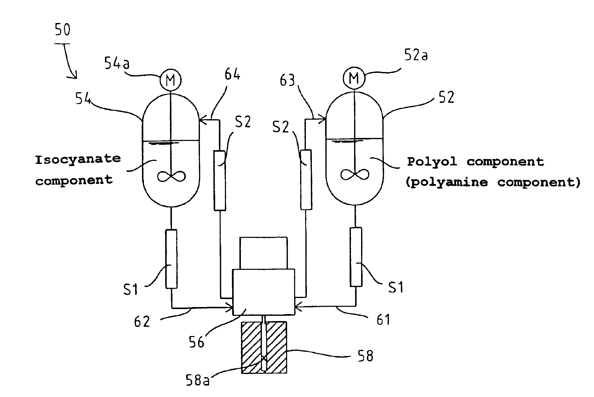
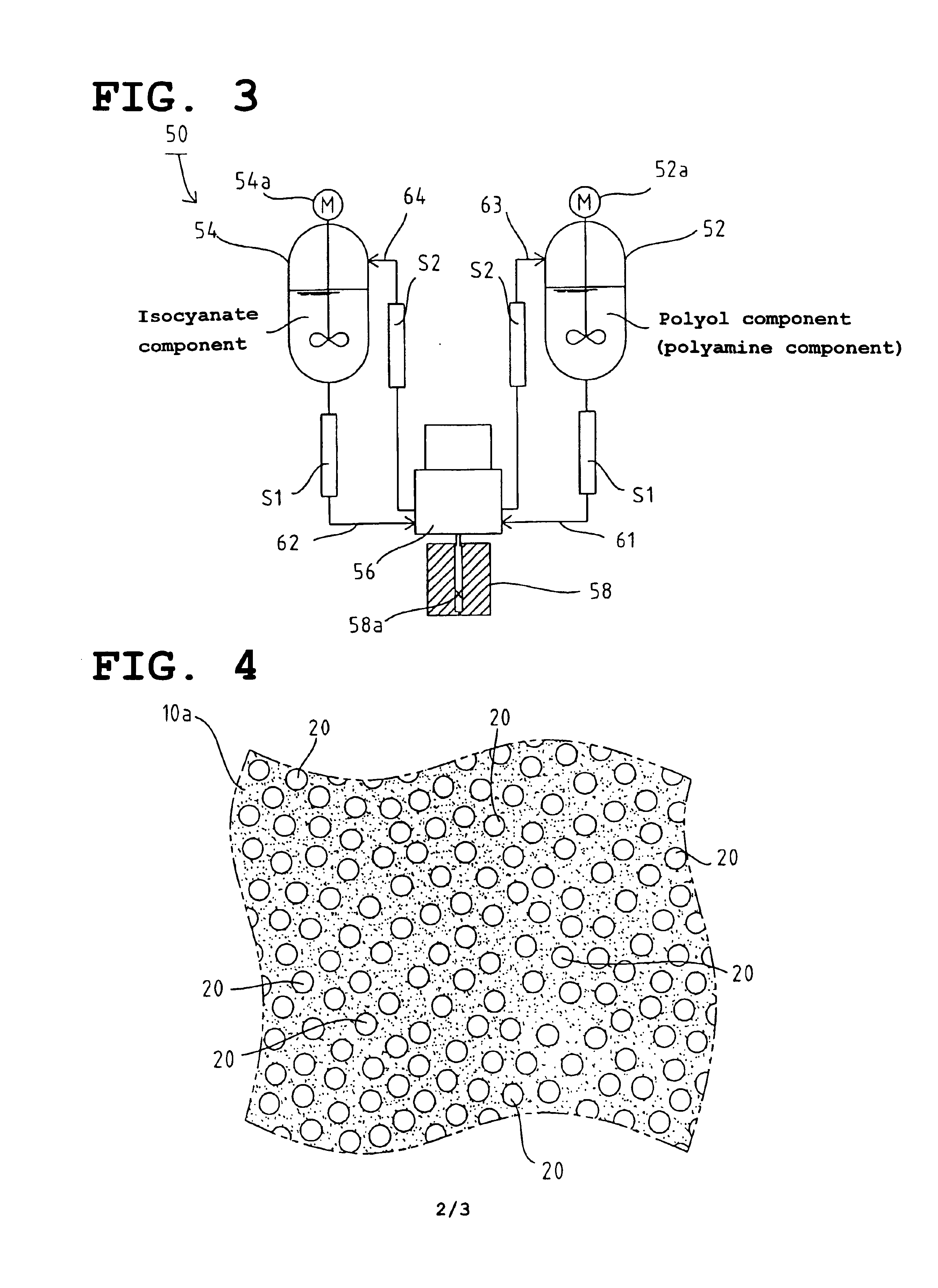
The polishing pad according to the invention will be further described hereinafter with reference to preferred embodiments. The inventors found that when a gas-dissolved raw material obtained by dissolving an inert gas in a polyurethane-based raw material is formed by a reaction injection molding method while arbitrarily controlling physical properties such as hardness, cell diameter and density, a polyurethane-based foam which can be preferably used as a polishing pad that is resistant to change of polishing conditions, can maintain an excellent removal rate and step height reduction. The inventors also found that the use of an aromatic diamine for example as a crosslinking agent makes it possible to inhibit the change of viscoelasticity depended on the temperature of the polyurethane-based foam.

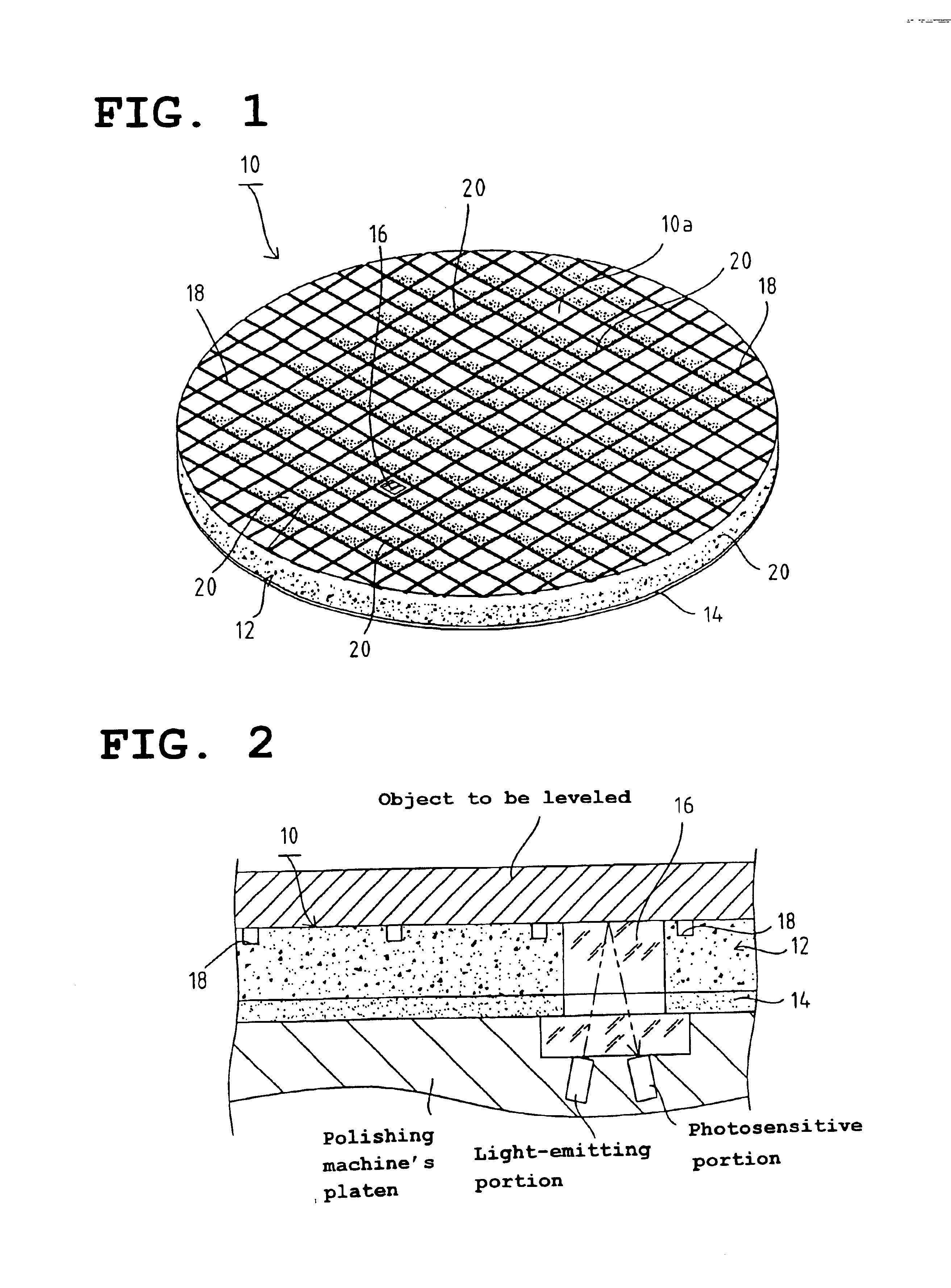
As shown in FIG. 1, the polishing pad 10 according to the present embodiment is in the form o...


PUM

PropertyMeasurementUnit
Temperatureaaaaaaaaaa
Pressureaaaaaaaaaa

Abstract

A high quality polishing pad suitable for chemical mechanical polishing (CMP) of semiconductor wafer, etc. which is not affected by the change of polishing conditions during polishing and can attain excellent removal rate, capacity of step height reduction and uniformity is described, wherein a polyurethane-based foam 12 having fine and uniform cells 20 suitable for polishing of semiconductor material, etc. obtained by reaction-injection molding a gas-dissolved raw material prepared by dissolving an inert gas in a mixture of a polyurethane or polyurea as a main raw material and various subsidiary raw materials under pressure is used.

Description

FIELD OF THE INVENTIONThe present invention relates to a polishing pad and more particularly to a polishing pad suitable for chemical mechanical polishing (CMP) which can polish a member having high requirements for precision and surface flatness such as semiconductor wafer.BACKGROUND OF THE INVENTIONOne of the important technologies supporting the recent rapid technical progress is the development of information technology, such as the computer. It is not too much to say that the development of performance of the aforementioned information technology can be attained by the development of performance and integration of the CPU (central processing unit) of information engineering equipment, i.e., ULSI (ultra large scale integrated) device constituting CPU. As one of the methods for drastically developing the performance and integration of ULSI devices, a method has been practiced which comprises developing the horizontal integration of ULSI, i.e., finely dividing elements, while deve...

Claims


Application Information

Patent Timeline
IPC IPC(8): B24D3/20B24D3/26B24B37/04B24D13/00B24D13/14B24B37/20B24B37/24B24B37/26B29C45/00B29C45/37B29K75/00B29K105/04B29L31/00C08G18/00C08G101/00C08J5/14H01L21/304
CPCB24B37/24B24D3/26B24B37/26B29B7/7694B29B7/826C08J5/00
Inventor HISHIKI, SEIGO
Owner ROGERS INOAC CORP
Why Eureka
Try Eureka