

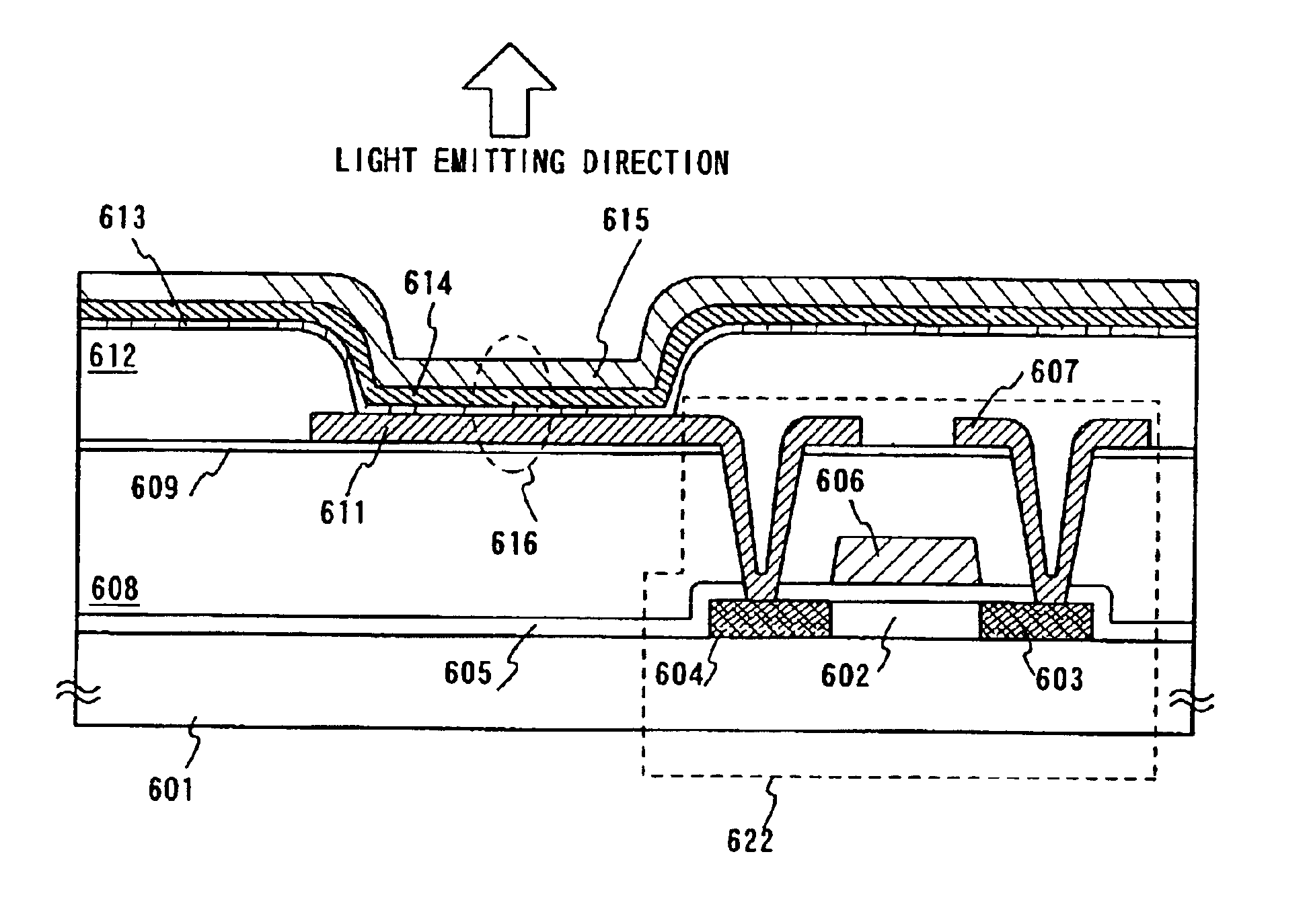
Light emitting device and manufacturing method therefor
a technology of light-emitting devices and manufacturing methods, which is applied in the direction of static indicating devices, discharge tubes luminescnet screens, instruments, etc., can solve the problems of limited opening ratio, complicated process, and light leakage on the substrate side, so as to simplify the process, reduce the cost, and widen the selection range of electrode materials
- Summary
- Abstract
- Description
- Claims
- Application Information
AI Technical Summary
Benefits of technology
Problems solved by technology
Method used
Image

Examples
embodiment mode 1
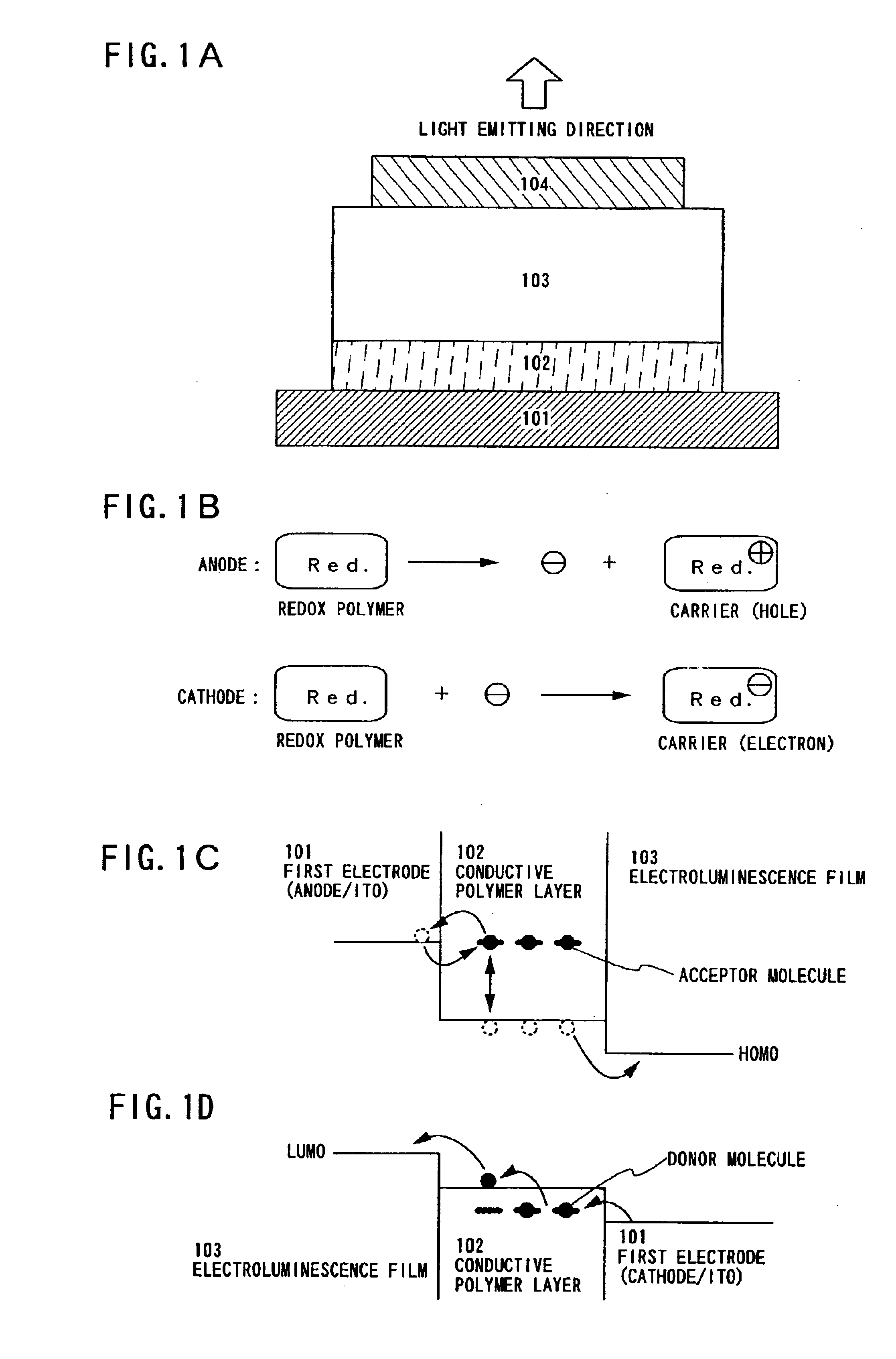
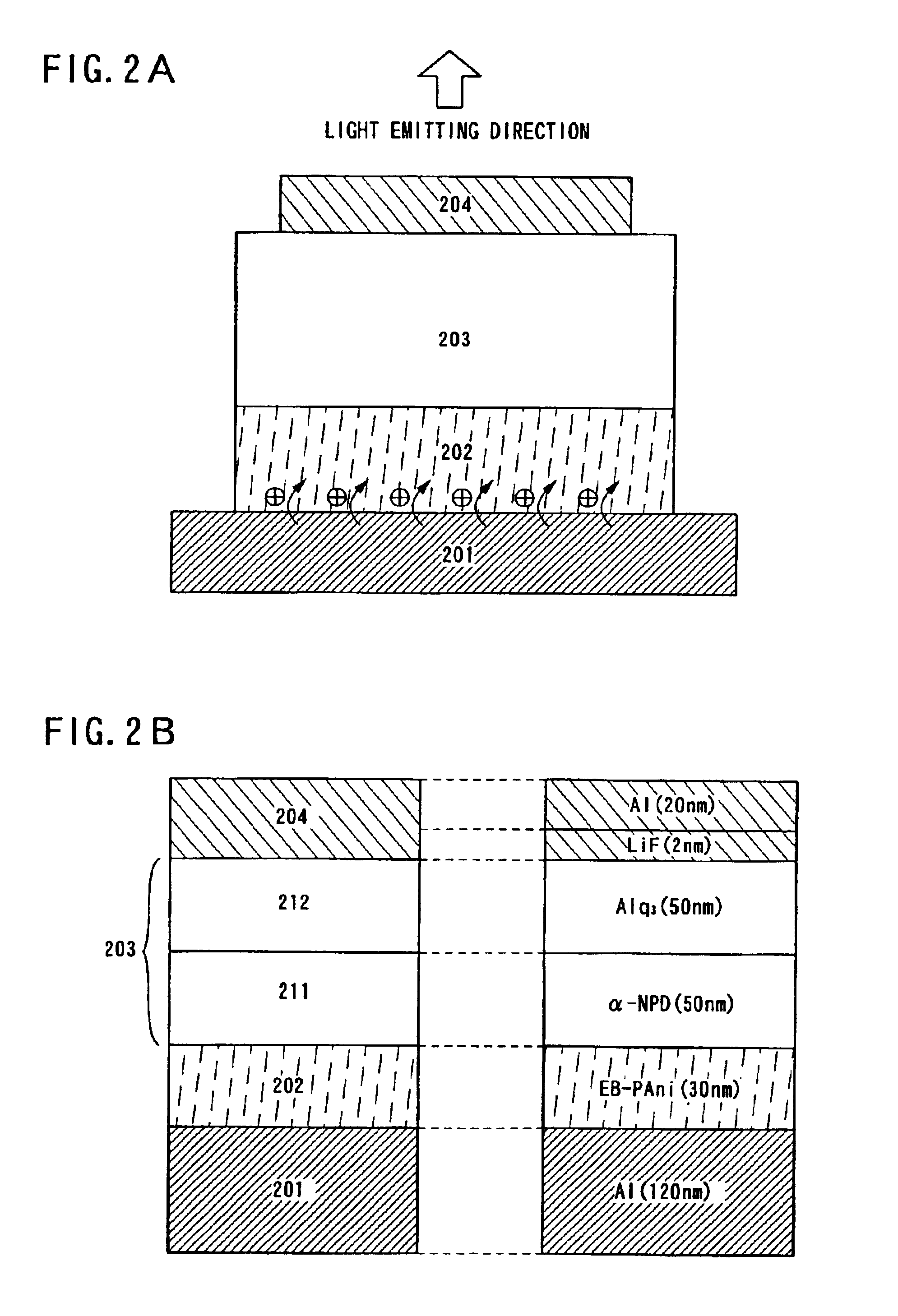
In Embodiment Mode 1, the case will be described with reference to FIG. 2 in that a redox polymer layer 202 made from redox polymer is formed as a conductive polymer layer on a first electrode 201, an electroluminescence film 203 on the redox polymer layer 202, and a second electrode 204 is formed thereon.
The first electrode 201 is usually formed from an anode material having high work function since the first electrode 201 functions as an anode, however, since the first electrode 201 is formed in contact with the redox polymer layer 202 in this embodiment, materials having high work function are not necessary to be used. It is preferable that a metal material is used that give the first electrode 201 light blocking effects or light reflecting effects. Specifically, Al can be formed to have a thickness of approximately 120 nm as shown in FIG. 2B.
The redox polymer layer 202 is formed on the first electrode 201. In addition, emeraldine base polyaniline (hereinafter, EB-PAni) can be us...
embodiment mode 2
In Embodiment Mode 2, the case in which a doping layer 302 that is polymer doped with dopant is formed as a conductive polymer molecular layer on a first electrode 301, and a second electrode 304 is formed thereon as shown in FIG. 3A will be described.
The first electrode 301 serves as an anode in Embodiment Mode 2 as well as Embodiment Mode 1. Materials for forming the first electrode 301 are preferable to have a high work function (specifically, materials having at least 4.0 eV work function).
Next, a doping layer 302 is formed on the first electrode 301. The doping layer 302 described in Embodiment Mode 2 is p-type, and made from polymer materials and dopant that is an acceptor molecule. Specifically, the doping layer 302 is made from polymer materials that polyethylenedioxythiophene (hereinafter, PEDOT) doped with polystyrene sulphonic acid (hereinafter, PSS) to have a thickness of 20 to 50 nm (preferably, 30 nm). Another known materials can also be used as polymer materials and d...
embodiment mode 3
In Embodiment Mode 3, the case in which a redox polymer layer 402 made from redox polymer is formed as a conductive polymer layer on a first electrode 401, an electroluminescence film 403 is formed thereon, and a second electrode 404 is formed thereon as shown in FIG. 4A will be described.
Serving as a cathode, the first electrode 401 is generally made from cathode materials with a low work function. However, since the first electrode 401 is formed in contact with the redox polymer layer 402, it is not necessary to use materials with a low work function. In the present invention, it is preferable that a metal material is used that give the first electrode 401 light blocking effect or light reflective effects. Specifically, Al can be formed as the first electrode 401 to have approximately a 120 nm thickness as shown in FIG. 4B.
The redox polymer layer 402 is formed on the first electrode 401. Further, the redox polymer layer 402 is made from EB-PAni to have a thickness of 25 to 50 nm (...
PUM
| Property | Measurement | Unit |
|---|---|---|
| Electrical conductor | aaaaa | aaaaa |
| Transparency | aaaaa | aaaaa |
| Electroluminescence | aaaaa | aaaaa |
Abstract
Description
Claims
Application Information