Silicon single crystal produced by crucible-free float zone pulling

a technology of crucible-free float zone and single crystal, which is applied in the direction of silicon compounds, under a protective fluid, transportation and packaging, etc., can solve the problems of unfavorable dislocation-free single crystals with a diameter of significantly more than 150 mm, and achieve the goal of avoiding electrical spark-over in the region of the coil supply conductor, and a wide range of difficulties

Inactive Publication Date: 2005-01-11
SILTRONIC AG
View PDF17 Cites 11 Cited by
  • Summary
  • Abstract
  • Description
  • Claims
  • Application Information

AI Technical Summary

Benefits of technology

Therefore it is an object of the present invention to provide a silicon single crystal by crucible-free float zone pulling which has a diameter which is considerably greater than 150 mm over a defined length and is free of dislocations in the region of this length, and also to provide a wafer which is separated from a single crystal of this type and a process for producing a single crystal of this type.
While previously the pressure of the gas atmosphere in the receptacle has been considered a relatively uncritical parameter, it has been found that the formation of a melt neck between the stock ingot and the product ingot (single crystal) takes place in a considerably more stable manner at pressures in the range from 1.5-2.2 bar (absolute pressure), particularly preferably in the range from 1.5-2.0 bar, than at higher pressures. It is thereby possible to ensure a stable flow of molten material to the single crystal. Lower pressures appear to be even more favorable but are not preferred within the scope of the present invention, since the high electrical power which is required to melt the stock ingot causes the risk of electrical spark-overs to increase greatly.
It is particularly preferred for the gas stream to be in the form of a laminar flow at least in the region of the side walls of the receptacle, in order to thin the contaminating substances and expel them from the receptacle. The gas stream therefore has a protective function for the interior of the receptacle, since the substances which are desorbed from the walls are entrained at the point where they are formed and are kept away from the melt.
A mixture of inert gas, preferably a mixture of argon and nitrogen, is proposed for use as the atmosphere in the receptacle. The favorable effect of nitrogen fractions in the atmosphere in connection with the suppression of electrical spark-overs and the prevention of what are known as swirl defects has already been mentioned in the prior art. With regard to the proposed continuous gas stream, optimum suppression of electrical spark-overs is achieved at a nitrogen concentration of 0.1-0.4% by volume. This quantity of nitrogen, which considerably reduces the likelihood of spark-overs, can, on account of the continuous stream of gas, be increased to this high level without nitrogen being incorporated in the silicon single crystal in a concentration of more than 2×10¹⁵ / cm3.

Problems solved by technology

Despite long years of experience gained using this technique, it has not hitherto been possible to pull dislocation-free single crystals with a diameter of significantly more than 150 mm.
This objective is confronted by a whole range of difficulties.
For example, relatively high electrical power is required to melt down the stock ingot, and consequently there is a particularly high likelihood of electrical spark-overs in the region of the coil supply conductors.
Another difficulty is that of achieving a dimensionally stable growth of the single crystal which leads to the appearance of the single crystal being as far as possible cylindrical.
This leads to misshapen single crystals which cannot be processed into wafers or can only be processed into wafers with difficulty.
However, the main problem is the considerable likelihood of dislocations forming.

Method used


Image

  • Silicon single crystal produced by crucible-free float zone pulling
  • Silicon single crystal produced by crucible-free float zone pulling
  • Silicon single crystal produced by crucible-free float zone pulling

Examples


example

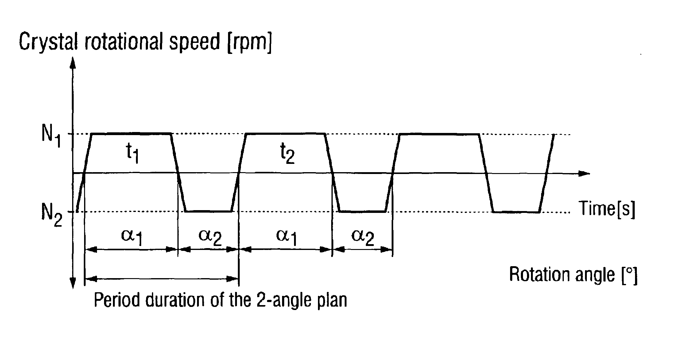
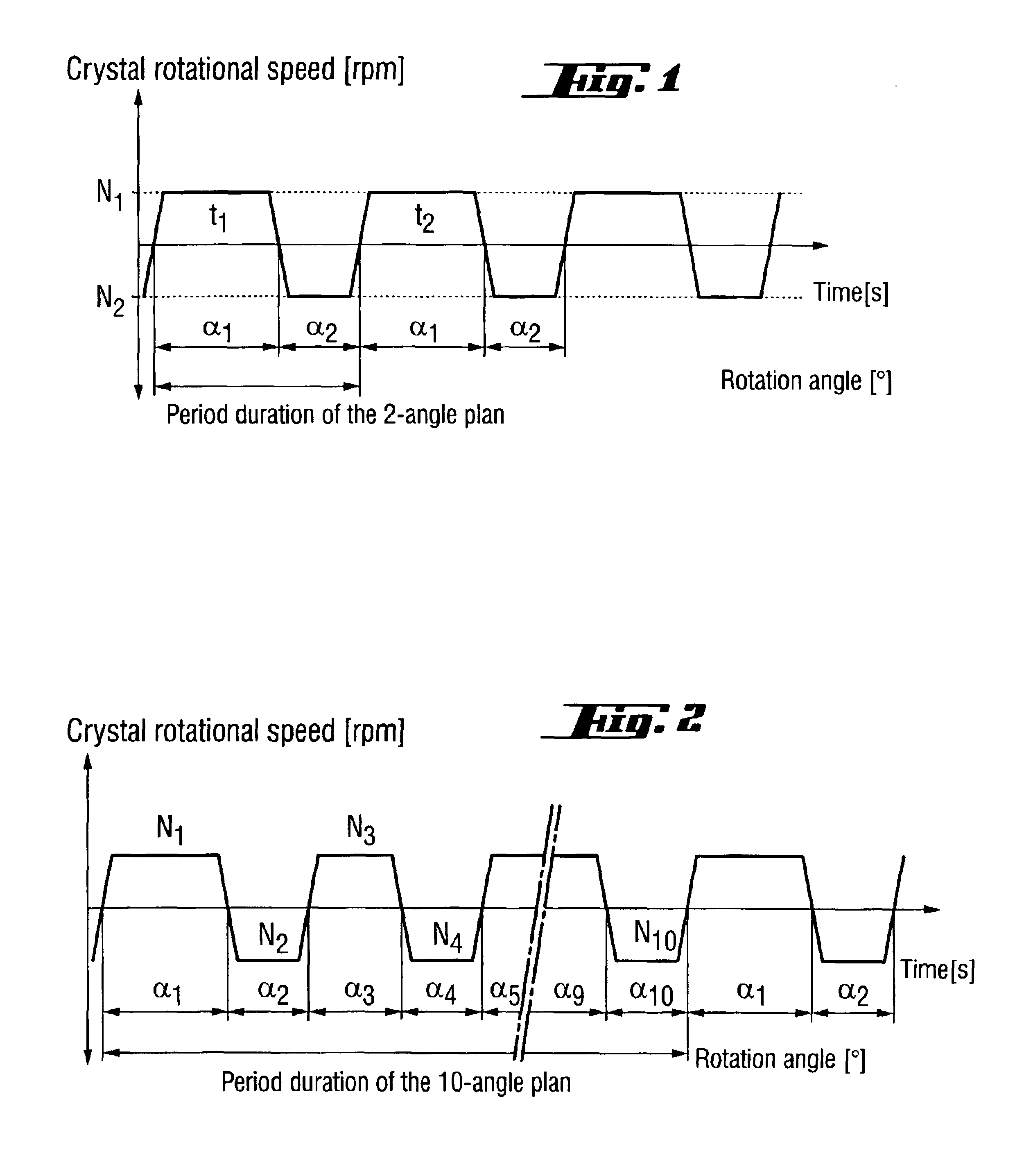
A silicon single crystal with a diameter of 204 mm, which was free of dislocations over a length of more than 200 mm, was pulled. In the preparatory phase, a polycrystalline stock ingot with a diameter of 155 mm was fitted into a receptacle. A seed crystal, a high-frequency coil designed as a flat coil (pancake coil) and a reflector for the single crystal were also provided in the receptacle. In a pumping phase, the receptacle was firstly evacuated and then filled with argon (1.65 bar) and nitrogen (0.3% by volume). Then, a gas mixture comprising argon and nitrogen was passed through the receptacle. The throughput was 4200 l / h s.t.p. (argon) and 13 l / h s.t.p. (nitrogen).

During a preheating phase, the stock ingot was heated on its lower end side, initially with the aid of a preheating ring and then by the high-frequency coil. After a molten droplet had formed on the seed crystal, the seed crystal was placed onto the stock ingot and the pulling of the single crystal was commenced, wit...


PUM

PropertyMeasurementUnit
lengthaaaaaaaaaa
diameteraaaaaaaaaa
external diameteraaaaaaaaaa

Abstract

A silicon single crystal is produced by crucible-free float zone pulling, has a diameter of at least 200 mm over a length of at least 200 mm and is free of dislocations in the region of this length. A silicon wafer is separated from the silicon single crystal by a process for producing the silicon single crystal. The silicon single crystal is produced by crucible-free float zone pulling in a receptacle, in which an atmosphere of inert gas and nitrogen exerts a pressure of 1.5-2.2 bar, the atmosphere being continuously exchanged, with the volume of the receptacle being exchanged at least twice per hour. A flat coil with an external diameter of at least 220 mm is inserted in order to melt a stock ingot. The single crystal is pulled at a rate in a range from 1.4-2.2 mm / min and is periodically rotated through a sequence of rotation angles. The direction of rotation is changed, after each rotation, by a rotation angle belonging to the sequence, a change in the direction of rotating defining a turning point on the circumference of the single crystal, and at least one recurring pattern of turning points is formed, in which the turning points are distributed on straight lines which are oriented parallel to the z-axis and are uniformly spaced apart from one another.

Description

BACKGROUND OF THE INVENTION1. Field of the InventionThe present invention relates to a silicon single crystal which is produced by crucible-free float zone pulling and has a large diameter.2. The Prior ArtPulling silicon single crystals by crucible-free float zone pulling (floating zone crystal growth, FZ pulling) is a technique which has long been known. In this technique, a polycrystalline stock ingot is gradually melted down with the aid of a high-frequency coil, and the molten material is converted into a single crystal by seeding with seed crystal in single crystal form and subsequently recrystallization. The principles of this process are described, for example, in DE-3007377 A.Despite long years of experience gained using this technique, it has not hitherto been possible to pull dislocation-free single crystals with a diameter of significantly more than 150 mm. This objective is confronted by a whole range of difficulties. For example, relatively high electrical power is requ...

Claims


Application Information

Patent Timeline
Patent Type & Authority Patents(United States)
IPC IPC(8): C30B13/00C30B13/26C30B29/06
CPCC30B13/26C30B29/06Y10T428/21
Inventor ALTMANNSHOFER, LUDWIGGRUNDNER, MANFREDVIRBULIS, JANIS
Owner SILTRONIC AG
Why Eureka
Try Eureka