Method of fabricating a magneto-resistive random access memory (MRAM) device

a random access memory and magnetoresistive technology, applied in the field of fabricating devices, can solve the problems of difficult to remove metal-containing residues, easy oxidation or damage, and short circuits within the mram film stack,

Inactive Publication Date: 2005-01-11
APPLIED MATERIALS INC
View PDF10 Cites 37 Cited by
  • Summary
  • Abstract
  • Description
  • Claims
  • Application Information

AI Technical Summary

Problems solved by technology

The MRAM film stack comprises materials that are sensitive to corrosion and may be easily eroded, oxidized, or damaged during device fabrication, as well as develop difficult to remove metal-containing residues.
The conductive residues or eroded layers may cause electrical short-circuits within the MRAM film stack.
Removal of such residues are time-consuming routines that decrease productivity and increase the cost of fabricating the MRAM devices.

Method used


Image

  • Method of fabricating a magneto-resistive random access memory (MRAM) device
  • Method of fabricating a magneto-resistive random access memory (MRAM) device
  • Method of fabricating a magneto-resistive random access memory (MRAM) device

Examples


Embodiment Construction

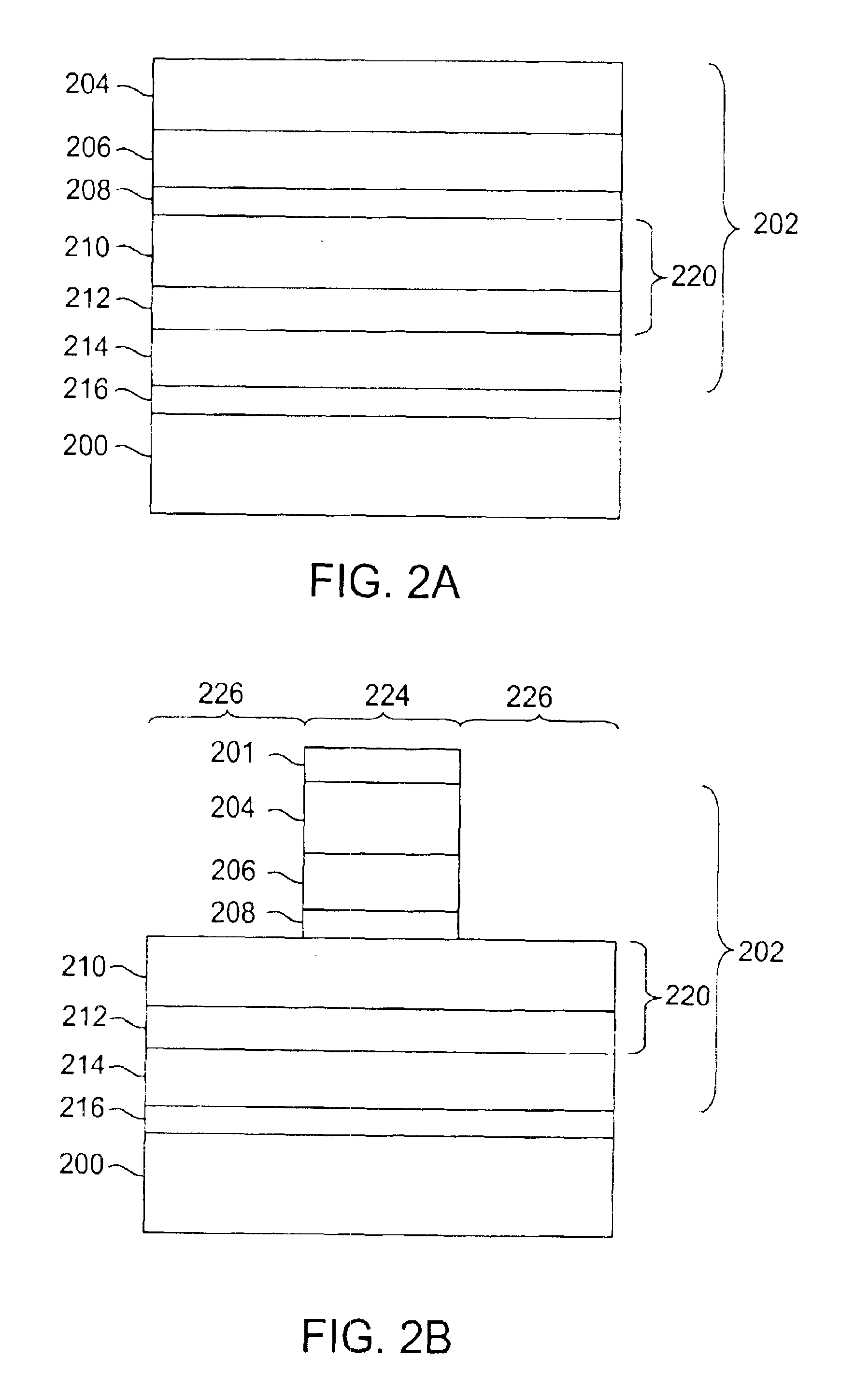
The present invention is a method of etching a multi-layer magnetic stack (e.g., layers of cobalt-iron alloy (CoFe), ruthenium (Ru), platinum-manganese alloy (PtMn), and the like) of a magneto-resistive random access memory (MRAM) device. Each layer of the multi-layer magnetic stack is etched using a process sequence including a plasma etch step followed by a plasma treatment step. The plasma treatment step uses a plasma comprising an inert gas to remove residues formed during the plasma etch step.

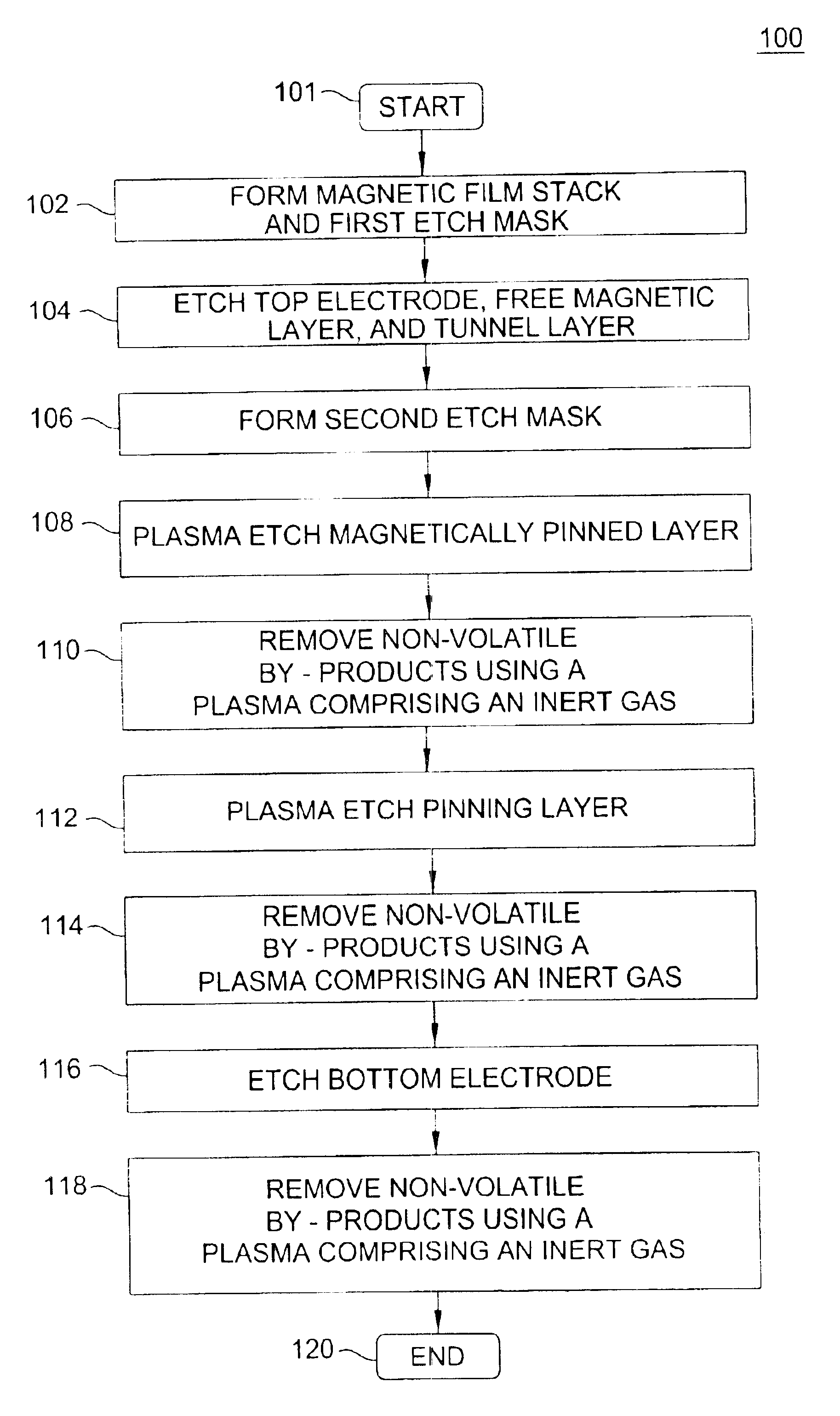
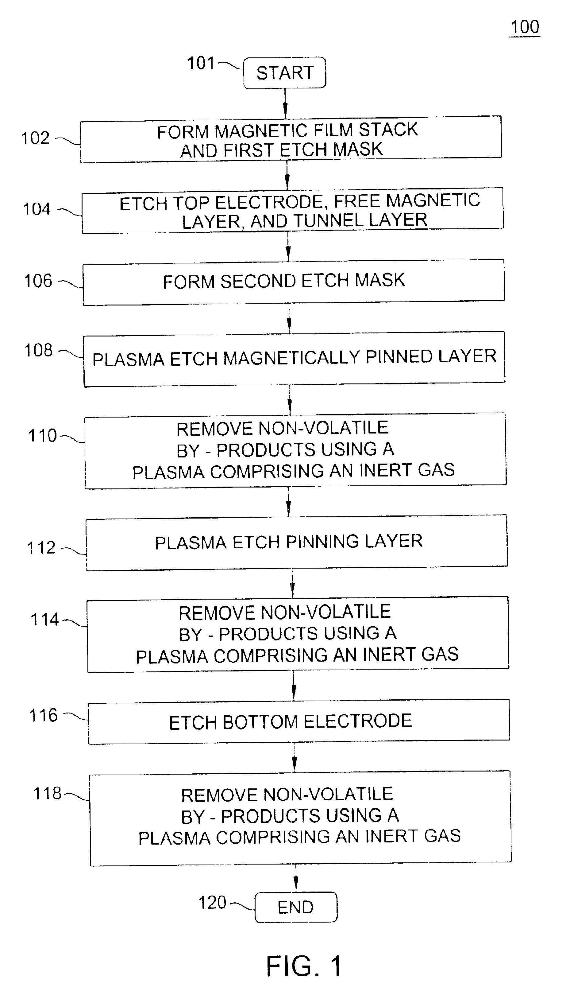
FIG. 1 depicts a flow diagram of one embodiment of the inventive method for etching the multi-layer magnetic stack of a magneto-resistive random access memory (MRAM) device as sequence 100. The sequence 100 includes the processes that are performed upon a magneto-resistive random access memory (MRAM) film stack during fabrication of such MRAM device.

FIGS. 2A-2I depict a series of schematic, cross-sectional views of a substrate comprising a MRAM device being formed using the sequence 100. T...


PUM

PropertyMeasurementUnit
chamber pressureaaaaaaaaaa
pressureaaaaaaaaaa
pressureaaaaaaaaaa

Abstract

A method of etching a multi-layer magnetic stack (e.g., layers of cobalt-iron alloy (CoFe), ruthenium (Ru), platinum-manganese alloy (PtMn), and the like) of a magneto-resistive random access memory (MRAM) device is disclosed. Each layer of the multi-layer magnetic stack is etched using a process sequence including a plasma etch step followed by a plasma treatment step. The plasma treatment step uses a plasma comprising an inert gas to remove residues formed during the plasma etch step.

Description

BACKGROUND OF THE INVENTION1. Field of the InventionThe present invention generally relates to a method for fabricating devices on semiconductor substrates. More specifically, the invention relates to a method for fabricating a magneto-resistive random access memory (MRAM) device.2. Description of the Related ArtMicroelectronic devices are generally fabricated on a semiconductor substrate as integrated circuits wherein various conductive layers are interconnected to one another to facilitate propagation of electronic signals within the device. An example of such a device is a storage element in memories such as magneto-resistive random access memories (MRAM) that facilitate storage of digital information.A memory cell in a MRAM device is a multi-layered structure comprising two sets of magnetic layers separated by a non-magnetic dielectric material. These layers are deposited as overlying blanket films, and then patterned to form the MRAM device. More specifically, the MRAM device c...

Claims


Application Information

Patent Timeline
Patent Type & Authority Patents(United States)
IPC IPC(8): H01L21/02H01L43/00H01L21/3213H01L43/12H01L21/3065C23F4/00H01F41/30H01L21/8246H01L27/105H01L43/08H01L43/10
CPCB82Y25/00B82Y40/00C23F4/00H01L43/12H01L21/02071H01L21/32136H01F41/308H10N50/01G09B9/042
Inventor YING, CHENTSAUCHEN, XIAOYIYAN, CHUNKUMAR
Owner APPLIED MATERIALS INC
Why Eureka
Try Eureka