Semiconductor devices and method for manufacturing the same

a semiconductor device and hetero junction technology, applied in the direction of semiconductor devices, transistors, electrical devices, etc., can solve the problems of deteriorating the characteristics of the transistor, large number of dislocations inherently present, and inability to expect the confinement of holes

Inactive Publication Date: 2005-01-18
PANASONIC CORP
View PDF20 Cites 53 Cited by
  • Summary
  • Abstract
  • Description
  • Claims
  • Application Information

AI Technical Summary

Benefits of technology

[0009]An object of the present invention is to take measures to suppress the problems as described above so as to provide a transistor having good characteristics while ensuring a sufficient reliability.

Problems solved by technology

Note however that since a hetero barrier is formed on the SiGe layer side, confinement of holes cannot be expected.
Moreover, a large number of dislocations inherently exist also in the Si channel layer formed thereon.
Such dislocations not only deteriorate the characteristics of the transistor, but also present a problem in terms of long-term reliability.
Thus, the device is very defective.
Moreover, such an SiGe buffer layer for lattice relaxation is required to have a considerable thickness (1 μm or more), whereby the crystal growth takes a long time, thus presenting a problem also in terms of throughput.

Method used


Image

  • Semiconductor devices and method for manufacturing the same
  • Semiconductor devices and method for manufacturing the same
  • Semiconductor devices and method for manufacturing the same

Examples


first embodiment

[0094

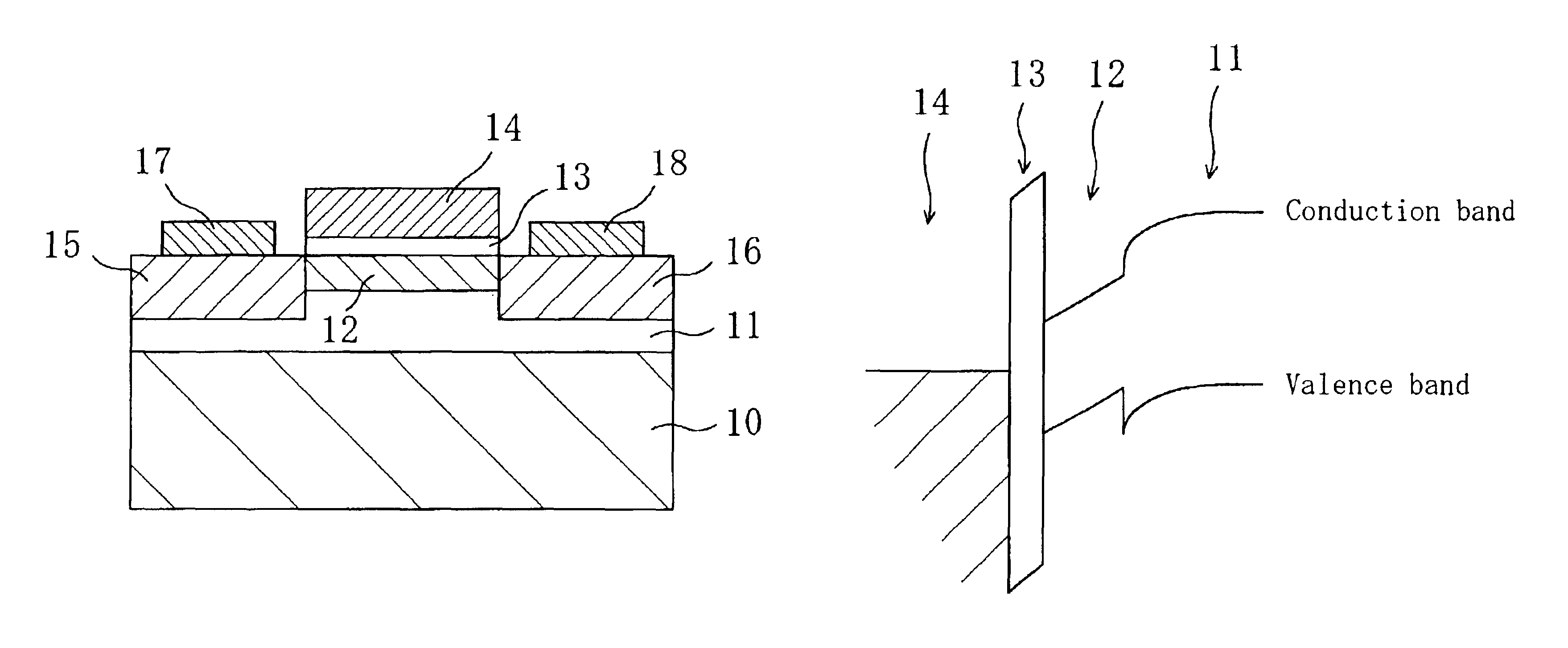
[0095]FIG. 1 is a cross-sectional view illustrating a structure of an n-MISFET in which tensile-strained silicon containing carbon is used as a channel according to the first embodiment of the present invention.

[0096]A substantially intrinsic Si layer 11, an SiC (Si1-yCy) channel layer 12, which is a silicon layer containing carbon, a CN gate insulating film 13 made of a carbon nitride layer (CN), which is a nitride, and a gate electrode 14 are deposited in this order on a p-type Si substrate 10. The Si layer 11, the SiC channel layer 12 and the CN gate insulating film 13 are all deposited by using an UHV-CVD method. Herein, it is preferred that the thickness of the SiC channel layer 12 is set to a value that is less than or equal to the critical thickness so that a dislocation due to a strain does not occur according to the carbon content. In the present embodiment, the carbon content of the SiC channel layer 12 is 2% (y=0.02), and the thickness of the SiC channel layer 12 is ...

second embodiment

[0104

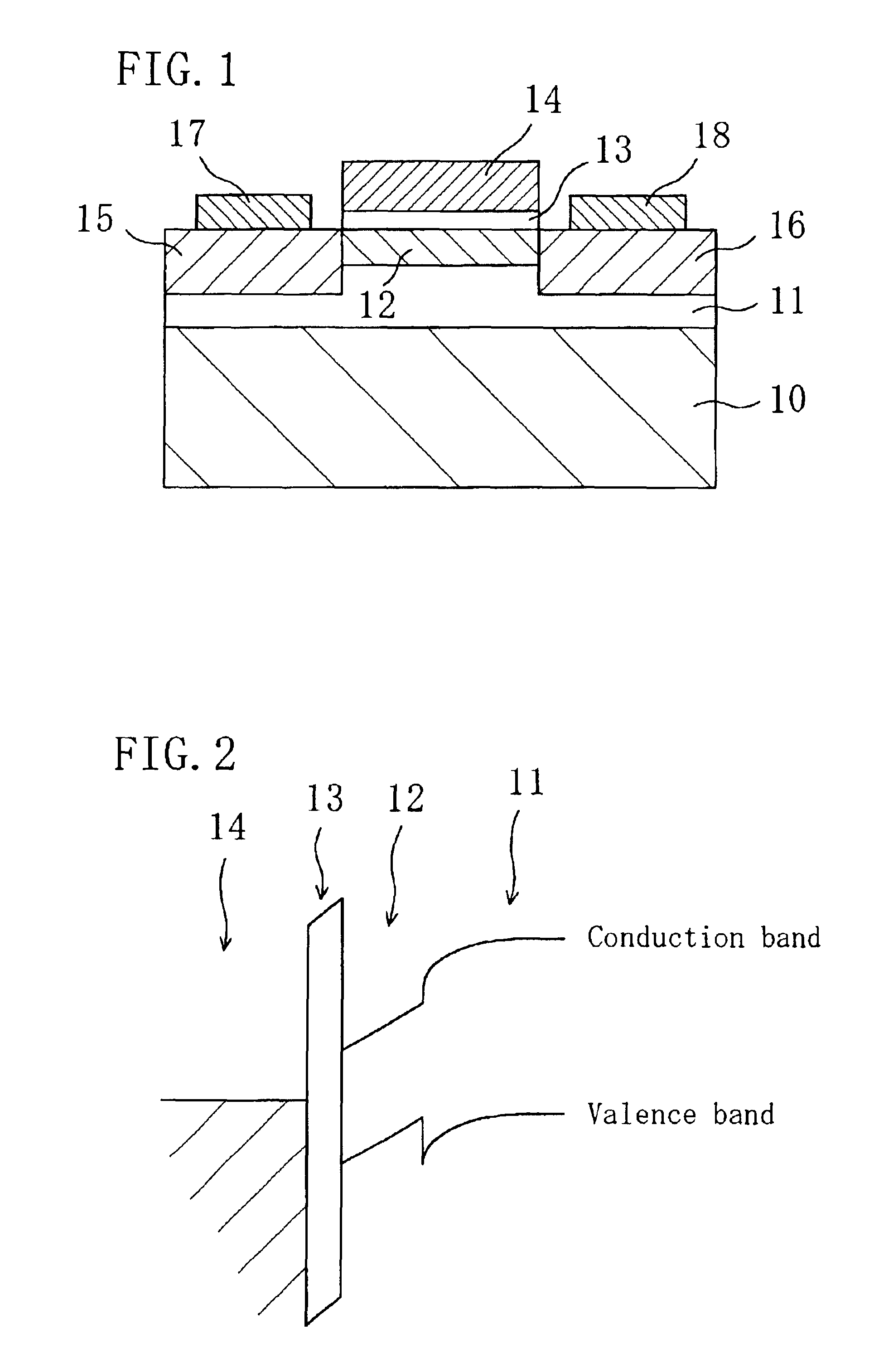
[0105]FIG. 3 is a cross-sectional view illustrating a structure of a p-MISFET in which tensile-strained silicon containing carbon is used as a channel according to the second embodiment of the present invention.

[0106]A substantially intrinsic Si layer 21, an SiC (Si1-yCy) channel layer 22, which is a silicon layer containing carbon, a CN gate insulating film 23 and a gate electrode 24 are deposited in this order on an n-type Si substrate 20. The Si layer 21, the SiC channel layer 22 and the CN gate insulating film 23 are all deposited by using an UHV-CVD method. Herein, it is preferred that the thickness of the SiC channel layer 22 is set to a value that is less than or equal to the critical thickness so that a dislocation due to a strain does not occur according to the carbon concentration. In the present embodiment, the carbon content of the SiC channel layer 22 is 2% (y=0.02), and the thickness of the SiC channel layer 22 is 10 nm. A source region 25 and a drain region 26, w...

third embodiment

[0114

[0115]FIG. 5 is a cross-sectional view illustrating a structure of a complementary MISFET in which tensile-strained silicon containing carbon is used as a channel according to the third embodiment of the present invention.

[0116]An n-well 31 and a p-well 32 are provided on an Si substrate 30. A p-MISFET having substantially the same structure as that illustrated in FIG. 3 is provided on the n-well 31, and an n-MISFET having substantially the same structure as that illustrated in FIG. 1 is provided on the p-well 32. Moreover, the p-MISFET and the n-MISFET are electrically insulated from each other by a trench isolation insulating film 33.

[0117]Specifically, the Si layer 11, the SiC (Si1-yCy) channel layer 12, which is a silicon layer containing carbon, the CN gate insulating film 13 and the gate electrode 14 are deposited in this order on the p-well 32, substantially as in the structure illustrated in FIG. 1. Also in the present embodiment, the carbon content of the SiC channel l...


PUM

PropertyMeasurementUnit
effective massaaaaaaaaaa
thicknessaaaaaaaaaa
distanceaaaaaaaaaa

Abstract

In a field effect transistor, an Si layer, an SiC (Si1-yCy) channel layer, a CN gate insulating film made of a carbon nitride layer (CN) and a gate electrode are deposited in this order on an Si substrate. The thickness of the SiC channel layer is set to a value that is less than or equal to the critical thickness so that a dislocation due to a strain does not occur according to the carbon content. A source region and a drain region are formed on opposite sides of the SiC channel layer, and a source electrode and a drain electrode are provided on the source region and the drain region, respectively.

Description

TECHNICAL FIELD[0002]The present invention relates to a field effect transistor using a hetero junction, and particularly to measures to improve the performance thereof.BACKGROUND ART[0003]Currently, the mainstream type of transistor that is formed on a silicon substrate is a metal / oxide film insulator / semiconductor (MOS) type field effect transistor (MOSFET). As a method for improving the characteristics of such a MOSFET, a method of applying a tensile strain to an Si channel layer is reported in articles (J. Welser et al., “Strain dependence of the performance enhancement in strained-Si n-MOSFETs,” IEDM Tech. Dig. 1994, p.373. and K. Rim et al., “Enhanced hole mobilities in surface-channel strained-Si p-MOSFETs,” IEDM Tech. Dig. 1995, p.517). This is a method in which a thick SiGe buffer layer is grown on a silicon substrate, and the lattice of the SiGe buffer layer is relaxed, after which an Si channel layer is formed thereon. This is to increase the lattice constant of the SiGe ...

Claims


Application Information

Patent Timeline
Patent Type & Authority Patents(United States)
IPC IPC(8): H01L21/02H01L29/66H01L21/70H01L21/04H01L29/40H01L29/51H01L21/318H01L21/8238H01L21/82H01L27/085H01L29/80H01L27/092H01L29/24H01L29/02H01L21/28
CPCH01L21/28185H01L21/28202H01L21/318H01L21/8213H01L29/802H01L27/092H01L29/1054H01L29/518H01L29/66068H01L21/823807H01L21/28194H01L29/1608H01L21/0217
Inventor KUBO, MINORUICHIKAWA, YOASAI, AKIRAKAWASHIMA, TAKAHIRO
Owner PANASONIC CORP
Why Eureka
Try Eureka