

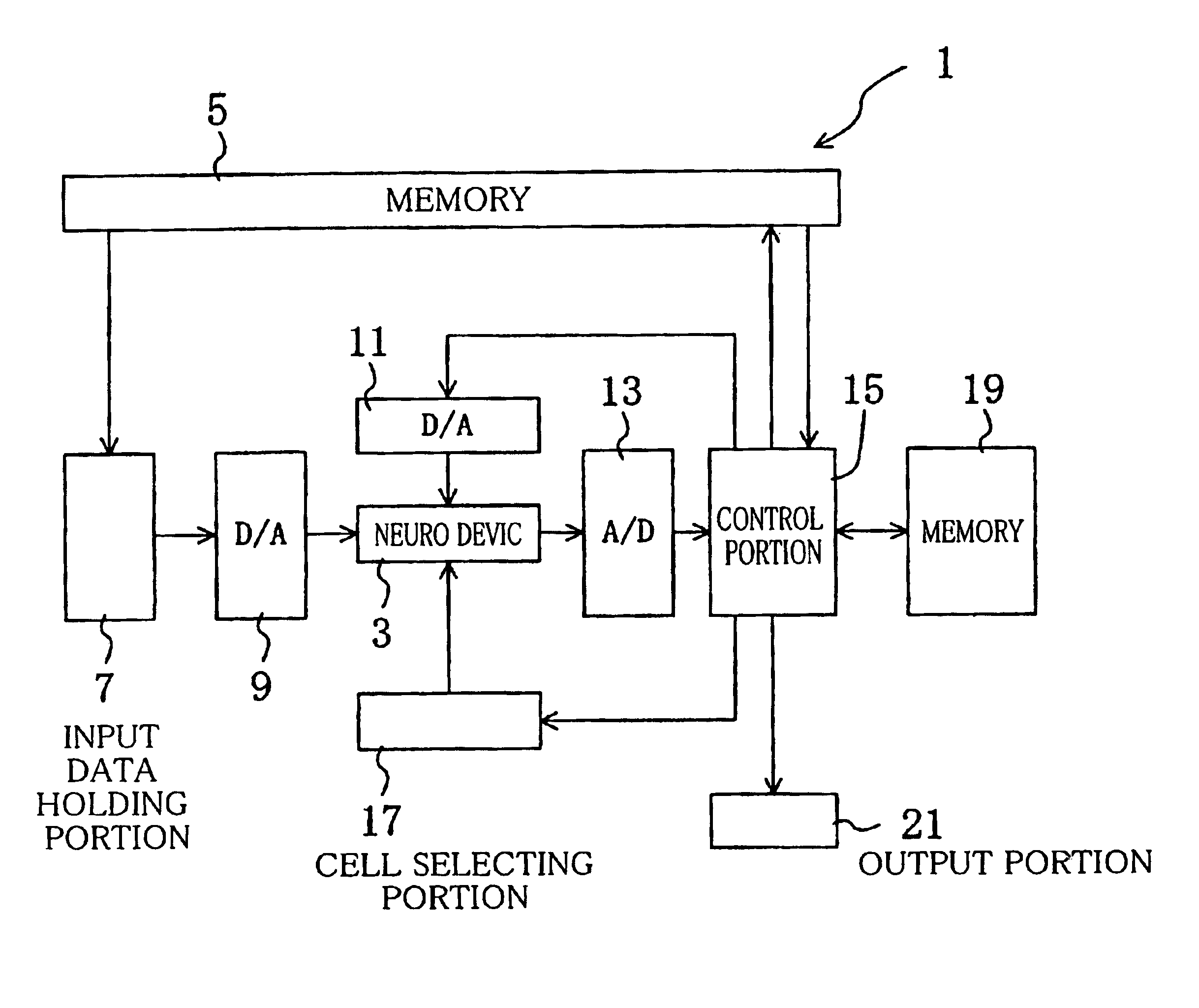
Semiconductor device and learning method thereof
a technology of mimiconductor and learning method, which is applied in the field of mimiconductor device and learning method thereof, can solve the problems of enormous time required for operation, relatively easy for human beings, and the tendency to increase in operation time, and achieve satisfactory operation speed and high reliability in learning
- Summary
- Abstract
- Description
- Claims
- Application Information
AI Technical Summary
Benefits of technology
Problems solved by technology
Method used
Image

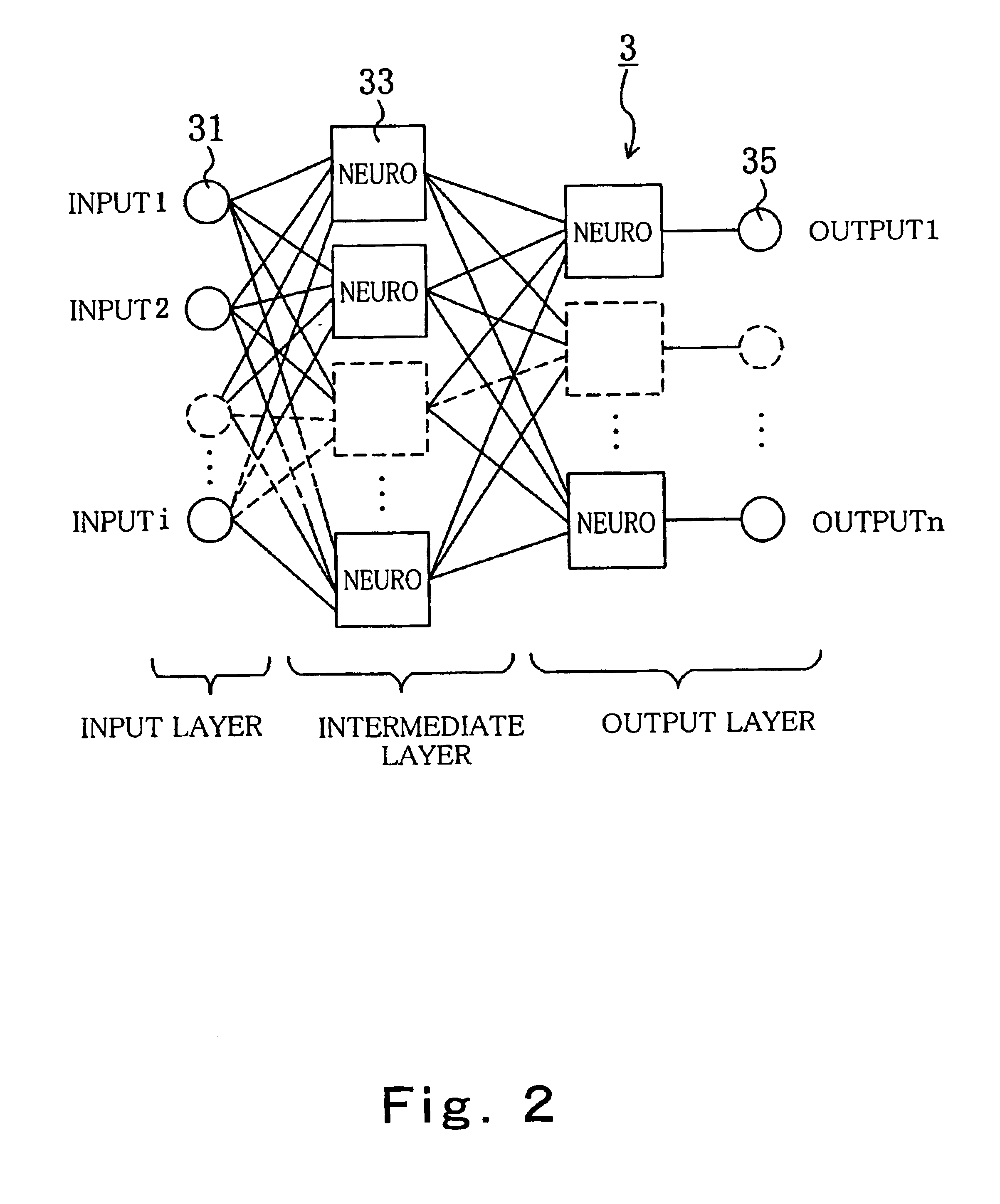
Examples
first embodiment
[Modification of First Embodiment]
A modification of the multiplier for use in the neural network system according to the first embodiment of the present invention will be described below.
FIG. 8 is a circuit diagram showing the modification of the multiplier for use in the neural network system of this embodiment.
As shown in FIG. 8, the multiplier of this modification is obtained by further providing a voltage-division adjusting capacitor 48 between the lower electrode of the ferroelectric capacitor 44 and a grounding conductor on the multiplier of described in the first embodiment.
In the multiplier of this modification, the voltage-division adjusting capacitor 48 is connected to the ferroelectric capacitor 44 in parallel with the PMIS 47 and the NMIS 49. Therefore, by adjusting a capacitance of the voltage-division adjusting capacitor 48, adjustment can be made so that a voltage given to the ferroelectric capacitor 44, a voltage given to the MIS capacitor present in the PMIS 47 and ...
second embodiment
(Second Embodiment)
A neural network system according to a second embodiment of the present invention is different only in structure of multiplier from the neural network system according to the first embodiment, and therefore, only the multiplier will be described.
FIG. 9 is a circuit diagram showing a configuration of the multiplier for use in the neural network system of this embodiment. As can be seen from FIG. 9, the multiplier of this embodiment is different in connection method of NMIS and PMIS from the multiplier according to the first embodiment.
As shown in FIG. 9, in the multiplier of this embodiment, a ferroelectric capacitor 81 is connected to a common gate electrode of a source follower circuit configured by NMIS 84 and PMIS 83. A source of the PMIS 83 and a source of the NMIS 84 are connected to each other and a substrate region of the PMIS 83 and a substrate region of the NMIS 84 are connected to each other. Further, the source of the PMIS 83 and the substrate region of...
third embodiment
(Third Embodiment)
A neural network system according to a third embodiment of the present invention comprises a multiplier using a phase-change memory technology.
FIG. 12 is a view showing a configuration of the multiplier included in the neural network system of this embodiment.
As shown in FIG. 12, a multiplier 121 of this embodiment comprises a first electrode 127a, a second electrode 127b, a resistance variable material 123 disposed between the first electrode 127a and the second electrode 127b, and a resistive element 129 connected to the resistive variable material 123. A switch 125d for ON / OFF controlling application of a weight voltage Vw is connected to the first electrode 127a. A switch 125a for ON / Off controlling application of an input voltage Vin is connected to one end of the resistive variable material 123. A switch 125b for controlling an output of an output voltage Vout is connected to a wire through which the resistive element 129 is connected to the resistance variab...
PUM
 Abstract
Description
Claims
Application Information